Tag Archive for: GaN

AOS (Alpha & Omega Semiconductor) has released a new Gallium Nitride device in their αGAN™ Technology platform: the AONV070V65G1.

The new device is a 650 V and 45 A device with a 70mOhm Rds(ON) (On-resistance). It’s the seconde device released by Alpha & Omega Semiconductor but it replaces the previous device. It’s proposed in a standard DFN 8×8 package.

Alpha & Omega Semiconductor has made the device available as of today, in production quantities, at a price of 8.00 USD for 10k units.

It comes to complete the power devices product line of Power MOSFET (including Super Junction MOSFET, IGBT, IPM, GaN and Power IC).

Datasheet: http://www.aosmd.com/res/data_sheets/AONV070V65G1.pdf

TDK-Lambda has been working on this product almost a year. The release has been delayed several times due to design issues to be solved before having a reliable and high quality product. PFH500F-28 has been released in November, without a great press and marketing shout outs. It was displayed at Electronica 2018, with no sign advertising for GaN devices inside, as one would expect. This is the first application of GaN power devices in this type of power supplies in module form factor.

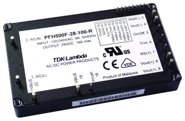
TDK-Lambda 500W power supply using Transphorm GaN devices for the PFC stage

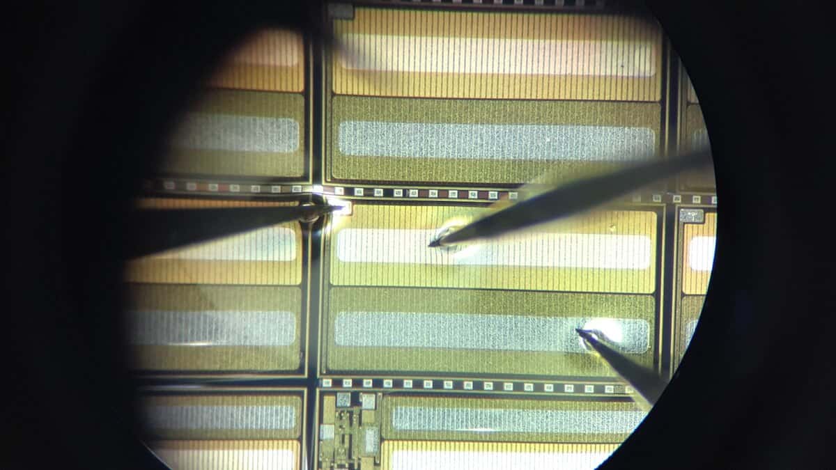
About the inside, TDK-Lambda used GaN transistors in a ‘bridge-less’ PFC stage. This delivers an efficiency of 98% for this stage, resulting in a peak efficiency of 92% for the overall power supply. The advantages of GaN transistors here is not only on efficiency but also on form factor: These power supplies are made to stay small and very flat. TDK says they have been able to reduce the board space by 25% thanks to GaN devices in this case. They target a limited amount of small volume industrial applications, where customers prefer to outsource the power supply stage and focus on their added value.

According to the marketing team at TDK-Lambda, the power supply could have been more efficient, at the cost of more components counts, a higher price, and potentially a bigger form factor due to limited board space. The GaN components used are from Transphorm (cascode D-Mode devices), that can provide the high switching speed necessary, together with the expected reliability.

The PFH500F is targeting off-the-shelf power supply markets as LED signage, communications, broadcast, test and measurement according to TDK.


Specifications:

  • Input: 85 to 265Vac
  • Output: 22.4 to 33.6V with 18A at 28V
  • PMBus control for output adjustment.

TDK says other output voltages will be available later this year.

We expect other manufacturers as Recom, or Cosel (through their recent acquisition PRBX) to release similar power supplies based on GaN devices in a near future. The market volume for such power supplies is quite small but still an opportunity for GaN to grow and show its used and reliable.

More info

Anker is a very well known leader for cheap USB-C cables, chargers for smartphones and laptops, and battery solutions to charge electronics on-the-go. As all players in this field, they work on size reduction and power density. As electronics become smaller and it seems power supplies struggle in following the same path.

Anker held a product presentation event in New-York, where they presented their latest products. One of these being the Atom PD1. It’s a 27W USB-C charger with a very small form factor and the following specifications:

  • Total Output Wattage: 27W
  • Input: 100 – 240V ~ 1.2A 50 – 60Hz
  • Power Delivery Output: 5V – 3A / 9V – 3A / 15V – 1.5A / 20V – 1.1A
  • Size: 1.61 in x 1.37 in x 1.49 in (4.1 cm x 3.5 cm x 3.8 cm)
  • Weight: 2.2 oz (62 g)

Anker claims it’s using GaN power devices, in order to reach such form factor and density. No information has been given about who is supplying devices for this charger, and we do not have a ASRP for this product. We, at PntPower, extensively promised Gallium Nitride power devices would be used in chargers. We still believe it’s going to be the one market segment to kickstart production. We expect now to see more and more high-end chargers with a small form factor being released. It will help and build the base of a steady production need for commercial GaN power devices.

iGaNPower, (GaN Power International) a GaN start-up based in Vancouver, Canada, has announced they designed and succeeded in manufacturing a first E-mode GaN high electron mobility transistor with a 1200V breakdown voltage.

This start-up is not part of the most visible GaN start-ups on the market today. It’s based in Canada, but seems to be part of Midea group, a Chinese electrical appliance manufacturer. They already have available devices, according to their website: 650V devices, in TO-220 or DFN 6×8, from 10 to 30 Amps, all shown as available (2 months leadtime), or even “in stock”.

Source: http://iganpower.com/news/

Transphorm Inc. today announced availability of its third generation (Gen III) 650-volt (V) GaN FETs. Power transistors built on Gen. III technology yield lower electromagnetic interference (EMI), increased gate noise immunity, and greater headroom in circuit applications.

The latest evolution of Transphorms’ devices, Gen III, to be released include the TP65H050WS 50 mΩ FET and TP65H035WS 35 mΩ FET, both available in standard TO-247 packages. Technologically, the incorporation of a new MOSFET along with other design modifications enable Gen III devices to deliver:

  • An increased threshold voltage (noise immunity) to 4 V from 2.1 V for Gen II, eliminating the need for a negative gate drive.
  • A gate reliability rating of ±20 V; an 11 percent increase versus Gen II.

As a result, switching is quieter, and the platform delivers performance improvement at higher current levels with simple external circuitry.

Regarding learned design techniques, Transphorm published elegant solutions for oscillation suppression in its app note 0009: Recommended External Circuitry for Transphorm GaN FETs. Example recommendations include the use of DC-link RC snubbers and switching-node RC snubbers that add further stability without adverse impact on efficiency. Notably, the solutions can benefit half-bridge and bridgeless totem-pole PFC topologies.

“It’s important to us to evolve our GaN technology based on customer need and real-world experience. Our Gen III FETs exemplify what’s possible when we adhere to that basic philosophy,” said Philip Zuk, Vice President of Technical Marketing, Transphorm.

Gen III 650 V Product Line Details:

Availability: Currently shipping

  • TP65H050WS 50 mΩ TO-247 unit price: 8.86 USD (sold in 1000 unit quantities)
  • TP65H035WS 35 mΩ TO-247 unit price: 11.55 USD (sold in 1000 unit quantities)

Optimal output ratings: 1.5 kW to 5.0 kW applications depending on design criteria

Source

VisIC Technologies, a Gallium Nitride (GaN)  power semiconductors start-up based in Israel, announced that it has closed $10 million in a Series D round of financing lead by a private investor.

“The insulated thermal pad is another welcome feature enabling the increase of the power stage reliability and density. Ultimately, 1200V rated GaN devices might be an attractive alternative in the 1200V segment dominated by SiC technology today.”

VisIC’s technology offering in combination with ongoing R&D designs by large players in the power electronics industry, made it possible to close this round of funding on favorable terms.

“We are very excited by the level of enthusiasm of VisIC’s investor, who believes in the enormous potential of VisIC’s GaN products. With the new funding, we can expand our portfolio further to address more market segments. Furthermore, we will increase our technical support team to assist our growing worldwide customer base.” said Tamara Baksht, VisIC Technologies’ founder and CEO.

Source

The French start-up Exagan, based in Grenoble and Toulouse, is launching its G-FET power transistors and G-DRIVE intelligent fast-switching solution, featuring an integrated driver and transistor in a single package. The firm claims that the GaN-based devices are easy to design into electronic products, paving the way for fast chargers that comply with the USB power delivery (PD) 3.0 type C standard while providing exceptional power performance and integration.

Exagan is showcasing the use of its high-power-density GaN-on-silicon devices to create ultra-fast, efficient and small 45-65W chargers, including demonstrating its electrical-converter expertise and how both the G-FET and G-DRIVE can benefit new converter product designs and their applications.

“The market potential for our products is enormous including all portable electronic devices as well as homes, restaurants, hotels, airports, automobiles and more,”

reckons president & CEO Frédéric Dupont. “In the near future, users will be able to quickly charge their smart phones, tablets, laptops and other devices simply by plugging a standard USB cable into a small, generic mobile charger.”

The ability of USB type C ports to serve as universal connections for the simultaneous transfer of electrical power, data and video is leading to tremendous growth.

Aiming to accelerate the power electronics industry’s adoption of cost-effective GaN-based solutions for the charger market, Exagan uses 200mm GaN-on-Si wafers, achieving highly cost-efficient high-volume manufacturing. The firm is now sampling its fast, energy-efficient devices to key customers while ramping up production to begin volume shipments of G-FET and G-DRIVE products.

Source

Infineon Technologies AG is starting volume production for CoolGaN™ products by the end of 2018, the company announced during PCIM Europe 2018 edition. Engineering samples of the high reliable GaN solution in the market are available now.

“Infineon is the global leader in power solutions and we truly believe that the next big thing in power management is gallium nitride,”

said Steffen Metzger, Senior Director High Voltage Conversion at Infineon. “Our goal is to be the first choice for customers when it comes to GaN power, and we have all assets in place to live up to this ambition. The market for GaN has been gaining a strong momentum; the advantages of using this technology in certain applications are evident. From operating expense and capital expenditure reduction, through higher power density enabling smaller and lighter designs, to overall system cost reduction, the benefits are compelling.”

Full production of CoolGaN 400 V and 600 V e-mode HEMTs will start by end of 2018:

  • CoolGaN 400 V will be available in 70 mΩ in SMD
    • Bottom-side cooled TO-leadless
    • Top-side cooled DSO-20-87 package
  • CoolGaN 600 V comes in
    • Top-side cooled DSO-20-87 package
    • Bottom-side cooled DSO-20-85.

The portfolio will be complemented with 70 mΩ and 190 mΩ 600V CoolGaN devices in bottom-side cooled TO-leadless  and DFN 8×8 packages with190 mΩ, the 600V CoolGaN portfolio will be complemented.

Source

Efficient Power Conversion (EPC) has announced the EPC2050, a 350V GaN transistor with a maximum RDS(on) of 65 mΩ and a 26A pulsed output current. Applications include EV charging, solar power inverters, motor drives, and multi-level converter configurations, such as a 3-level, 400 V input to 48 V output LLC converter for telecom or server power supplies.

The EPC2050 is 1.95 mm x 1.95 mm (3.72 mm2) integrated a half bridge with gate drivers. It occupies five times less area than a comparable silicon solution, using the usual Wafer-Level Package (WLP) used by EPC corp. for all their devices. EPC’s 350V transistor can handle thermal conditions more efficiently than plastic packaged MOSFETs, according to the company.

“The performance and cost gap of silicon with eGaN technology widens with the 350 V, EPC2050, that is almost 20 times smaller than the closest silicon MOSFET.”

said Alex Lidow, EPC’s CEO.


EPC2050 350V GaN device transistor half bridge

The EPC9084 development board is a 350V maximum device voltage, half bridge featuring the EPC2050, and the Silicon Labs Si8274GB1-IM gate driver. This 51mm x 38 mm board is designed for optimal switching performance and contains all critical components for easy evaluation of the 350 V EPC2050 eGaN FET.

The EPC2050 eGaN FET is priced for 1K units at $3.19 each and the EPC9084 development board is priced at $118.75 each from Digikey.

GaN Systems, the Canadian Gallium Nitride power transistor start-up, revealed during APEC 2018 conference in San Antonio, TX, its new product line. GS-010-120-1-T is an enhancement mode GaN-on-Si power transistor with a rated breakdown voltage of 100V, and a current capability of 120A, with a 5 mOhm Rdson. It surpasses the 90A of the latest GaN Systems high current device.

GaN Systems target the 48V applications in automotive, industry and renewable energy applications. Using 48V bus is quite a new trend pushed by form factor reduction needs, especially for automotive applications: Battery charging, BMS, auxiliary systems or small EV, as demonstrated recently by Valeo.

GaN Systems plans to develop technology solutions on these two main voltages: 100V and 650V, to target new applications and innovation spreading in this field.

Source

Navitas Semiconductor today announced that GaNFast™ power ICs are used in the ‘Mu One’, a universal 45W consumer charger with an ultra-slim form factor: 14mm thickness. A Navitas GaN power IC is used in combination with USB-PD (USB Type C plug). The 45W adapter can fast-charge a smartphone or charge a laptop.

GaN power ICs reduce the size, weight and cost of  passive components by operating at higher frequency, and keeping losses low. The use of such devices using GaN ICs was expected for more than a year. Precedents small and light chargers include Dart from FiNSix, Zolt from Avogy, or the 55cc from Innergie (a subsidiary of Delta Electronics). PntPower analyzed the trend in previous articles (here, here and here) and will soon publish an update on this topic.

This time, the device is produce by Made in Mind, a UK based start-up:

“At Made in Mind, we are pre-programmed to challenge industry norms, we seek the finest of partners who share our beliefs. The Navitas GaNFast chips in the Mu One gave us a tremendous edge on speed-of-charging, efficiency and size”.

Commented Mathew Judkins, CEO of Made-in-Mind.

“Consumers can anticipate a wide range of fast-charging, high-density solutions in the coming months as our customers deliver a new class of power adapters with our GaNFast power IC technology.”

said Gene Sheridan, Navitas CEO.

The Mu One 45W adapter is available via a crowdfunding campaign, similarly to its competitors.

Panasonic developed a new gate technology for GaN Power Devices. The insulated-gate transistor allows a continuous stable operation with no variation in its threshold voltage. It’s called MIS, for Metal Insulated Semiconductor. While continuing to improve and produce its GaN GIT, Panasonic worked on this new type of GaN devices based on MIS gate structure. Hysteresis normally occurs in MIS type GaN devices. Here, Panasonic managed to obtain continuous stable operation, which is required to operate the devices at high frequency.

They announced a few of the characteristics:

  • Continuous stable operation: maximum gate voltage of +10V
  • Drain current: 20A
  • Breakdown voltage: 730V
  • OFF operation time of 1.9 ns and ON operation time of 4.1 ns

A mix of Panasonic previous GaN technology, and gate structure innovation

The transistor is based on some previously developed and proven innovation from Panasonic as their GaN-on-Si technology. This allows the breakdown voltage of 730V. They also developed a crystal growth process to from the recessed gate structure without defects or processing damages. This allows the normally-off operation with such a drain current capability.

Source: Panasonic

The new gate insulator is based on AlON (Aluminum Oxynitride). It suppresses the hysteresis phenomenon usually observed for such a gate structure, created by electron traps within the insulator.

No production or commercialization roadmap has been given.

Source