I recently had the chance to test drive a Tesla. Not like any Tesla, the super-powered one: S85PD.
The one that has an “Insane” mode and can beat a Ferrari at traffic lights. Even though there was no Ferrari at the traffic light we stopped at, I can trust the fact that it can compete with many supercars.
And as a power electronics market analyst, I had to ask the sale guy about inverter and power modules. He did not know much about that. It’s not really his job, and he is not a design engineer. He knew a lot about the car and its features (which is enough to sell it) but not about the inside of the inverter, the power train, or the car…
So I asked Siri Google, and I had answers. I ended up on a Tesla car owners forum. I looked into it, and I found pictures and description of the inverter. Like the the picture down here.

Fig.1: 2×14 IGBTs in parallel is one leg of inverter—All packaged in discrete TO247 – From Tesla Roadster and Model S inverter
All about Tesla and power semiconductor packaging
That’s the truth. Don’t go for a reverse engineering on a Tesla inverter. Engineers just made an awesome car with very simple off-the-shelf products. Do not look for any highly special package for power modules International Rectifier (now-Infineon) would have made specially for Elon Musk (just because he is Elon Musk). There is no such thing. The inverter is made of TO-247 packages (Figure 1), derived from TO-220 in the 1990’s in order to handle more power and heat.
They used 20-year-old power module packaging technology to build the fastest electric luxury car on earth. It’s that simple.
I was shocked again! (The first shock was experiencing the acceleration of “Insane” mode.) I wanted to share that with someone. So I went on the internet and asked a very dumb question on the Power electronics group of LinkedIn.
A question that sounded like that:
And many comments, questions and reactions (and “likes”. There are “likes” in LinkedIn too… But you cannot “poke” anyone. I wish we had that feature).
And for those of us who are not hanging out in this virtual professional world of LinkedIn, I wanted to summarize discussions here.
What you get from these discussions
1. “Module or discrete?” is still a 2015 question.
The first power module packaging design question is to know if you are going to use a power module or not. And that is a question that Tesla engineers had to ask themselves and that JB Straubel, CTO of Tesla, asked himself designing the model S. He talked about it during 2010 APEC conference, and I wish I was there :-(
But according to the attendees, the choice of going for TO-series package rather than well-marketed EV series of power modules were:
- Simplicity of assembly
- Heat dissipation (and thus easy cooling)
Which is in total accordance to any engineer mind designing a product to:
- Work
- Be efficient
As the rest of the design is not engineering work … most of the time.
2. Power modules & IGBT packaging preconception
Most comments agree on the fact that a power module is a great thing, with a lot of room for innovation and many great features.
But they also agree on the fact that there are other factors to think about, when going for a design in power electronics, depending on the applications.
You still need to think about:
- Volumes of production
- Total cost of the solutions
- Heat spreading and cooling requirements
- Peak currents, ripples and other EMC stuffs
- Size
Still you have interesting feedback putting down some preconception on power modules:
- “The TO series are indeed very tough little beasts and I have been told by a senior semiconductor reliability engineer in some ways more reliable than a module, with respect to bond wires. Not something they usually advertise as the same company also makes modules targeted at EV/HEV”
- “The TO-series package are really quite outstanding and I’ve used them a lot”
- “That design allows Tesla to ‘insanely’ run 1500A through the inverter IGBTs and then the motor”
3. Theories on why Tesla made unexpected IGBT packaging choices
For most of the participants in the discussion, the choice of TO-247 totally made sense, but not always for the same reasons:
It could be because:
- “The design was done when they were not sure about the volumes”
- “There was no suitable module available at that time” (then what about today?)
- “They wanted to reduce the risk of failure for this new product”
The point is not actually to try to find the right one, but to think about it.
We are in 2015, and we still find so many reasons why discrete TO-247 packaging could be a very good choice.
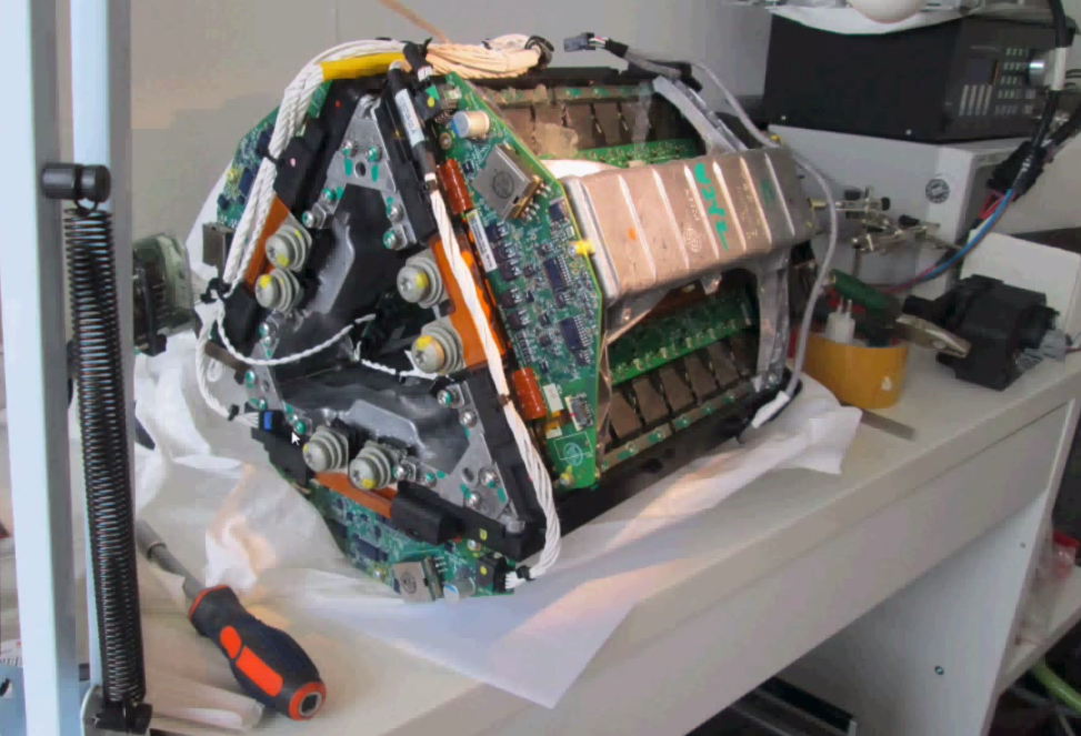
Tesla Model S inverter – 3 phase represented by the triangle, having each two switches of 14 IGBTS in parallel
4. Power module packaging for EV/HEV—What’s next?
The state of the art and what would be the best choice in the future has also been discussed.
An interesting comment points out that:
the state of the art in power device packaging […] will most probably be in the higher volume, mass manufactured electric vehicles—from Ford, Toyota, GM, etc., There are definitely higher performance packages—with better characteristics in terms of thermal, inductance, tolerance to vibration, etc.
or that:
Tesla might not have the volume to drive custom power electronics packaging.
Which totally makes sense and proves that Toyota has a huge knowledge of how to build a power converter and hybrid car. They started Prius back in 1994 and have all the feedback and experience since then. On the other side, and that is Point The Gap comment: Is power electronics for Hybrid cars and Power electronics for full electric cars the same thing?
You get rid of a lot of constraints, starting with space and cooling restrictions when you design for a full electric car. (e.g.: Tesla’s cars have a rear and front trunk, with batteries under the car and inverters/motor group not taking much space).
4.1 .XT, SKiN and other IGBT packaging innovations
There is also a reminiscence of .XT Technology (Infineon) and SkiN (Semikron). These two technologies have been in one of our articles about PCIM 2015.
From Point The Gap point of view, these are all very interesting innovations. It’s just that they have been presented 2 to 4 years ago, and we are still waiting for available products. Remember the marketing campaign from Semikron in 2013 about SKiN technology. According to them, it may be ready in 2016. Why so much communication 3 years before availability…
And finishing with something that sounds very true to us:
“According to Tesla’s website the Power Electronics Module uses 84 IGBTs to power the 3-phase induction motor, or 14 IGBTs in parallel per switch. Is it the best solution? I seriously doubt it, although it may be the ‘lowest cost’ solution based solely on the bill of materials.”
4.2 Is best power semiconductor packaging “no-packaging”?
A parallel discussion also emerged on discrete packaging innovations. You must know EPC’s WLP (Wafer Level Package). The innovation here is that there is no package. The die has a protection coating on one side and bumps on the other. No wires, no wire bonding issues.
Of course this reduces the risks of failures. But as pointed in a comment: “Chipscale packages/no-packages are exciting at lower voltage and power for converters, power supplies, etc., but PCB interconnects bring back resistance and inductance.” An affirmation that is disputed by no-package manufacturers.
Conclusion: Join the conversation
If you have comments on this, join us in the group. We would be happy to have your feedback. It’s an interesting discussion.
Sources: http://insideevs.com/; https://teslamotorsclub.com

