
The question is: Who really needs GaN or SiC Power Devices ?
We know that GaN and SiC are a recurring topic, and you may be overwhelmed with it. We are sorry but what has been said about Gallium Nitride (GaN) and Silicon Carbide (SiC) power devices’ market in the past hasn’t done much good to the Power Electronics community. At PntPower.com, we want to be talk openly about what is happening. So here is our point of view.
The question is: “Who really needs GaN or SiC Power Devices?”
We’re not the kind of analyst to go through the usual message about WBG and how they are awesome and will change the world. Yes, the technology is interesting. But we strongly believe it’s not about the performances, it’s about the product/market fit. So the only question we need to ask ourselves is: What do GaN and SiC bring to power electronics systems, that IGBT, MOSFET and Super Junction MOSFET don’t?
We worked on applications-oriented market reports in order to start answering this tricky question. The idea was to define the market segments where GaN brings a real competitive advantage (not only performance-based, any competitive advantage). What we learned was: many market segments will be open to GaN penetration only when prices drop. GaN devices manufacturers may say otherwise to try and sell a wonderful world with GaN everywhere, but many applications are too cost-driven to ever be interested.
It’s quite the same story for Silicon Carbide. The technology has been here for a while, but it took time for the right product to find the right market. And that fit happened on a much higher voltage than the current product offering. So potential users had to be patient. The market estimations produced in the early days of SiC looked very optimistic for a while, now they are more reliable (only a few years later).
GaN Power Devices and SiC Power Devices’ market penetration cannot be compared
We know you had many market reports trying to tell you about this marvellous competition between the two Wide Band Gap materials, GaN and SiC. But why would GaN and SiC be in competition on the Power devices market when one gives its best at 10 kV (or so) and the other at 0.6kV (600V)? These power devices simply do not compare, and so don’t their market penetration. We cannot measure different technologies on a similar scale when they bring different advantages.
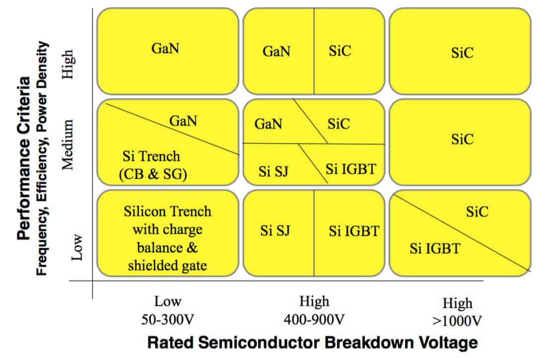
Extract from a Fairchild Semiconductor presentation. Designed originally by Alex AVRON, founder of PntPower.com
GaN is fit for lower voltages, high-end products. It is in direct competition with Super Junction MOSFET, when SiC is in competition with IGBT. The only voltage range SiC and GaN share could be 600V in the kilowatt range applications. But in this voltage range, we believe that GaN will quickly be cheaper than SiC, and there will be no competition. So there’s no huge fight coming up: we’re pretty sure that only one technology perfectly fits your needs.
There is a possibility that GaN reaches good performances up until 1200V later, so that’s something that could move the lines a bit in the future. But we’ll see…
Now what do the end-users and system designers feel about SiC and GaN: enthusiasts? In the end, they’re the only ones who will validate the product/market fit. The replies we had from the people we interviewed were very different from one application to another and the whole analysis is synthesized in our market report.
Teaser: the main idea is that the first market segment to adopt GaN will be the consumer applications segment.
GaN Power Devices is for Consumer markets first, and SiC will be for Transportation markets
Wide Band Gap power devices are not cheap, so the benefit of using them rather than another (cheaper) technology has to be huge. What would be that benefit, and could it be important enough to make the cost a secundary criteria? Years ago, Super Junction MOSFETs brought smaller and more efficient power supplies to consumer applications. This tendency to value size and efficiency for a device has not slowed a bit, it has even become a huge deal in the consumer market. A deal worth value, thus a deal that makes GaN interesting, despite its higher cost. Innovation is driven by high-end side.
Many have been struggling to define what the future application for Silicon Carbide MOSFET will be. The SiC material characteristics provide devices with a very high-blocking voltage (much higher than GaN, MOSFET and even IGBT). This characteristic makes it very attractive only for a limited type of application. These applications, such as rail traction or Grid and T&D, are already working on R&D development for these devices. But these segments also have very long product lifecycles (35 years for rail traction!), which makes production introduction and adoption very long.
When one technology leads to the consumer market, and the other one to complex industrial markets, we can bet that market penetration and trends will not be very similar.
The Next Steps for SiC & GaN in Power Electronics
Don’t expect Wide Band Gap to be quickly adopted in the power electronics world. Those things take time. For human reasons, for technology reasons, for money reasons. But if you want to know better what will happen for GaN in power electronics, we have a market report for that.
Curious about the SiC market? We plan on releasing an online training in 2018. Meanwhile, you can write us a message with your questions and we will give you an answer.


There has been some activity in GaN today with GaN Systems, EPC and others. but I don’t see where they are being implemented.
where are their major design wins?
Hi Andrew,
The implementation of GaN takes a little bit of time, and it will start with niche makets. We cannot really see major design that would obviously integrate GaN. Even the laptop/electronics charger market has design improvements possible without GaN. I think that Dialog Semiconductor, main supplier for Apple power conversion parts, releasing a GaN IC for chargers is a good sign.
Gan allows higher power density so you’ll see thinner tv’s, smaller devices. There is slow adoption partially because alot of the big companys dont want to compete with themselves so they’re taking a wait and see. Kind of like electric cars, before Tesla came along. People will want lighter and smaller chargers and gan enables that. Also Gan products in 500-600 Volt have been achieved. It allows smaller passive devices like inductors and caps and companys are working on products to integrate the gan drivers into the same die to save BOM costs. This is attractive to companys.
Thanks for your comment. It’s a tiny, but clear explanation of where we are now. The question we try to reply to in our market reports and analyses is: “When, who and how will GaN be used ?”
I miss a true comparison of salient technical features. It is NOT true that GaN can replace and is superior to Si SJ! All GaN devices are destroyed by any overvoltage, it is even forbidden to test them because alsready the test is detrimental and kills the device. (See GaNSystems.) Any standard or SJ Si mosfet takes an enormous amount of overload by going into a non-destructive avalanche mode, Hence GaN devices can only be used in a limited number of circuit topologies where overvoltages do not occur (e.g. in PFCs).
Excessive marketing hype (“… Rdson orders of magnitude lower…”) has meanwhile fully subsided! To this date there is not a single GaN power device on the market which has a lower Rdson as the 2013 Infineon 650 V/19 mOhmmax product! The lowest GaN features in 2017 32 mOhmsmax. This is the truth.
The cascodes which are on the market with either GaN or SiC JFETs upstairs achieve their better performance from the cascode circuit and not from GaN or SiC. In a cascode, it is only the lower transistor, a standard Si mosfet , which determines the performance, upstairs it can be any, a hv fast bipolar or any Si mosfet will do as well.
Scrutiny of GaN data sheets will surface quite astonishing results: e.g. in one data sheet it is claimed “operating frequency > 100 MHz”. In the same data sheet, 4 pages further, the sum of rise, fall and delay times is given as 55 ns. Obviously, absolutely unfit for 10 ns period operation. And lo and see: all application circuits of this manufacturer operate at 100 to 133 KHz…
GaN and SiC JFETs do have advantages only in bridge circuits, not because they are made of GaN or SiC, but because they are JFETs. Si power JFETs were made some decades ago by 4 Japanese manufacturers, today there are none to my knowledge, so a comparison is not possible.
Other disadvantages like the much lower thermal conductivity of GaN, especially as lateral devices on Si substrates, are also seldomly mentioned.
Last, not least: there are quite a few unresolved problems with GaN like the socalled current collapse (onyl one of many) which causes destruction. Some claim that this was resolved , bus this must first be proven over the years. Some manufacturers with large GaN knowhow about hf transistors either never entered the GaN field (like Cree) or withdrew..
In contrast, SiC is firmly established and a solid technology which will grow exponentially in the coming transition to electric cars, because they beat Si IGBTs.
In the context of the use of this type of component in aeronautical equipment, the realibility is a major element of choice.
Do you have elements of comparison?
Can you clarify the maturity levels of each technology?.
Indeed, reliability can sometimes be a main concern. Even for mature technologies (IGBTs) we have seen in the past reliability issues on some series of components.
The subject is very sensitive in the power device manufacturing community, and for new technologies it’s very confidential. It’s very difficult to have access to trustworthy sources, both for us market analysts or for devices users. I think the best is to do your own research.
About maturity, it’s clear now that SiC 600V and 1200V has been here for longer than GaN 600V, and thus the SiC MOSFET technology can be clearly seen as more mature.
On the other side, GaN has moved from R&D lab to available samples very fast. It would not be surprising that the technology catches up.
From PntPower point of view, the choice must be made first on voltage, power and switching frequency that match your application. GaN and SiC will not play in the same field.
If you need help in identifying and benchmarking potential suppliers, we can help in this task.
Alex AVRON from PntPower
Any update on the online training for SiC? When will it be available?
Our planned release is Q4-2018. So you can expect to be up-to-date on SiC for Christmas! We will keep you (and everyone) posted.
I am newbie,i just wanted to the the cost or price differences between Gallium nitride and silicon carbide ?
Which is the cheaper between GaN and SiC and Si???