Tag Archive for: GaN

Transphorm, one of the best-known Gallium Nitride power electronics start-ups has officially opened its”Center of Excellence” in San Jose, California. A team was established and growing for one year in Silicon Valley. It’s now official. The Center will also have worldwide offices.

The objective was to support and educate customers about the GaN transistor technology and how to design using this new wide band gap material based devices. Center’s staff will also build a knowledge base made of white papers, reference designs and publications.

Transphorm, like many of its competitors, now needs to educate and evangelize the market. It’s required to accelerate adoption of GaN Devices, and avoid the long and slow adoption of SiC MOSFET we have seen for the past 5 years.

Navitas, innovating start-up in WBG semiconductor, has announced the release of the first fully integrated IC in Gallium Nitride. It’s based on their AllGaN transistor platform.

Navitas is targetting charging solutions, fast-chargers and small power high-end converters with this half-bridge building block. GaN based transistor are able to operate at much higher frequency, with lower losses than currently used solutions for these converters: Super Junction MOSFET.

GaN transistor Navitas half-bridge IC

The NV6250 is a 650V half-bridge with intergrated Navitas driver technology iDrive. It switches at up to 2Mhz, all packed in 6x8mm QFN package.

Production is planned for Q2 2017 (which is very soon…).

Navitas Semiconductor announced the immediate availability of production qualified iDrive™ Gallium Nitride (GaN) Power ICs using the company’s proprietary AllGaN™ technology. The NV6131, NV6105 & NV6115 offer a high-efficiency 650V, 160mOhm power FET with increasing integration of digital and analog circuits, leading to ground breaking speed, energy efficiency, power density and reduced system cost.

GaN can enable up to 100x higher frequencies than silicon but driving, controlling & protecting such high-speed power devices has been an industry challenge that has limited adoption.  By integrating these critical digital and analog circuits monolithically with the GaN power device, these system level problems have been eliminated. Navitas GaN Power ICs with iDrive guarantee optimized & robust performance for any application. A 10-100x increase in system operating frequency is combined with higher efficiencies to enable up to a 5x increase in power densities and 20% lower system costs.

“GaN Power ICs, with the monolithic integration of logic, analog & power, represent an industry breakthrough that will change the landscape of power electronics as we know it”, explained Navitas CEO Gene Sheridan.  “By integrating all gate-drive-related circuitry, virtually all frequency-related power losses are eliminated, opening the door to significant frequency and efficiency gains.  We anticipate a major upgrade cycle in mobile fast chargers, thin TVs, high-efficiency data centers, LED lighting, solar and electric vehicle markets as this new high-speed revolution in power electronics gets underway”, Sheridan added.

“The Center for Power Electronics Systems (CPES) at Virginia Tech has been pioneering the advancement of high-frequency power systems for over three decades” explains Dr. Fred Lee, the university’s distinguished and globally recognized professor. “The invention of GaN power ICs represents a major industry breakthrough and is a critical ingredient to make high-speed, high-efficiency power systems a reality.  This is an exciting time for the power industry”, Lee concluded.

VisIC Technologies, an innovator of efficient power electronics based on Gallium Nitride (GaN) semiconductors, announced today that it has closed $11.6 million in a Series C financing lead by a new investor Birch Investment with participation of existing investors.
The revolutionary potential of GaN-based electronics for electrical power delivery systems, from consumer power supplies to solar inverters, UPS, power supplies for Cloud/Data Centers and electric motor drives, has been marketed and anticipated for years, especially for high voltage and high current switching applications. VisIC Technologies is the company that demonstrated performance of high current GaN switching device and 1200V GaN power switch.

“We are very excited by the level of support provided by VisIC’s new and existing investors, who share our vision for the extraordinary potential of VisIC’s GaN based products. It is an important milestone for our company. Having achieved the best performance metrics for any GaN devices in the market, this new capital infusion positions us to accelerate commercialization and dominate the market segment.”

said Tamara Baksht, VisIC Technologies’ founder and CEO.

About VisIC Technologies:
Based in Nes Ziona, Israel, VisIC Technologies, Ltd. was established in 2010 by experts in Gallium Nitride (GaN) technology to develop and sell advanced GaN-based power conversion products. VisIC has successfully developed, and is bringing to market, high power GaN-based transistors and modules. (GaN is expected to replace most of the Silicon-based (Si) products currently used in power conversion systems.) VisIC has been granted keystone patents for GaN technology and has additional patents pending.
For more information:  www.visic-tech.com

Panasonic, which recently launched mass production of its X-GaN process of lateral GaN HeMT, presented a 1.7kV GaN device during IEDM conference. GaN devices available today are limited to 650V for enhancement mode devices, and 1200V for depletion-mode normally-on devices. Panasonic’s device demonstrated during IEDM is a GaN/GaN Vertical device having a Ron of 1mΩcm².

The device is based on a V-shaped structure, and a secondly grown GaN/AlGaN interface separated from the first one, which improves electron mobility by a factor of 5. Panasonic’s team also used a carbon doped GaN layer to avoid punch-through phenomenon.

Source

We know that GaN and SiC are a recurring topic, and you may be overwhelmed with it. We are sorry but what has been said about Gallium Nitride (GaN) and Silicon Carbide (SiC) power devices’ market in the past hasn’t done much good to the Power Electronics community. At PntPower.com, we want to be talk openly about what is happening. So here is our point of view.

The question is: “Who really needs GaN or SiC Power Devices?”

We’re not the kind of analyst to go through the usual message about WBG and how they are awesome and will change the world. Yes, the technology is interesting. But we strongly believe it’s not about the performances, it’s about the product/market fit. So the only question we need to ask ourselves is: What do GaN and SiC bring to power electronics systems, that IGBT, MOSFET and Super Junction MOSFET don’t?

We worked on applications-oriented market reports in order to start answering this tricky question. The idea was to define the market segments where GaN brings a real competitive advantage (not only performance-based, any competitive advantage). What we learned was: many market segments will be open to GaN penetration only when prices drop. GaN devices manufacturers may say otherwise to try and sell a wonderful world with GaN everywhere, but many applications are too cost-driven to ever be interested.

It’s quite the same story for Silicon Carbide. The technology has been here for a while, but it took time for the right product to find the right market. And that fit happened on a much higher voltage than the current product offering. So potential users had to be patient. The market estimations produced in the early days of SiC looked very optimistic for a while, now they are more reliable (only a few years later).

GaN Power Devices and SiC Power Devices’ market penetration cannot be compared

We know you had many market reports trying to tell you about this marvellous competition between the two Wide Band Gap materials, GaN and SiC. But why would GaN and SiC be in competition on the Power devices market when one gives its best at 10 kV (or so) and the other at 0.6kV (600V)? These power devices simply do not compare, and so don’t their market penetration. We cannot measure different technologies on a similar scale when they bring different advantages.

Silicon Carbide Gallium Nitride IGBT Super Junction MOSFET mapping market positionning and strategy

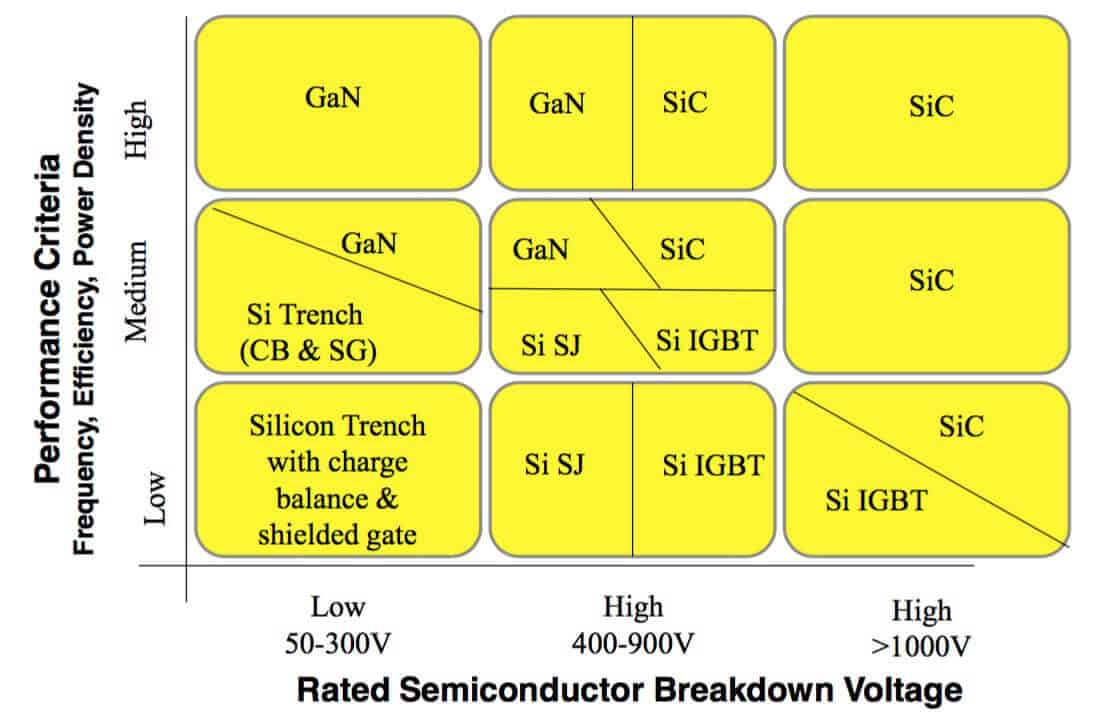
Extract from a Fairchild Semiconductor presentation. Designed originally by Alex AVRON, founder of PntPower.com

GaN is fit for lower voltages, high-end products. It is in direct competition with Super Junction MOSFET, when SiC is in competition with IGBT. The only voltage range SiC and GaN share could be 600V in the kilowatt range applications. But in this voltage range, we believe that GaN will quickly be cheaper than SiC, and there will be no competition. So there’s no huge fight coming up: we’re pretty sure that only one technology perfectly fits your needs.

There is a possibility that GaN reaches good performances up until 1200V later, so that’s something that could move the lines a bit in the future. But we’ll see…

Now what do the end-users and system designers feel about SiC and GaN: enthusiasts? In the end, they’re the only ones who will validate the product/market fit. The replies we had from the people we interviewed were very different from one application to another and the whole analysis is synthesized in our market report.

Teaser: the main idea is that the first market segment to adopt GaN will be the consumer applications segment.

GaN Power Devices is for Consumer markets first, and SiC will be for Transportation markets

Wide Band Gap power devices are not cheap, so the benefit of using them rather than another (cheaper) technology has to be huge. What would be that benefit, and could it be important enough to make the cost a secundary criteria? Years ago, Super Junction MOSFETs brought smaller and more efficient power supplies to consumer applications. This tendency to value size and efficiency for a device has not slowed a bit, it has even become a huge deal in the consumer market. A deal worth value, thus a deal that makes GaN interesting, despite its higher cost. Innovation is driven by high-end side.

Many have been struggling to define what the future application for Silicon Carbide MOSFET will be. The SiC material characteristics provide devices with a very high-blocking voltage (much higher than GaN, MOSFET and even IGBT). This characteristic makes it very attractive only for a limited type of application. These applications, such as rail traction or Grid and T&D, are already working on R&D development for these devices. But these segments also have very long product lifecycles (35 years for rail traction!), which makes production introduction and adoption very long.

When one technology leads to the consumer market, and the other one to complex industrial markets, we can bet that market penetration and trends will not be very similar.

The Next Steps for SiC & GaN in Power Electronics

Don’t expect Wide Band Gap to be quickly adopted in the power electronics world. Those things take time. For human reasons, for technology reasons, for money reasons. But if you want to know better what will happen for GaN in power electronics, we have a market report for that.

Curious about the SiC market? We plan on releasing an online training in 2018. Meanwhile, you can write us a message with your questions and we will give you an answer.

Infineon celebrated the Grand Opening of its new warehouse and Gallium Nitride (GaN) cleanroom at its Mesa facilityin Arizona, (USA). The multi-million-dollar expansion project added approximately 11,500 sq. ft. to the existing facility.

Dr. Juergen Woehl, Managing Director, Infineon Epi Services, said, “As a leader in semiconductor technology, our Mesa facility underlines Infineon’s commitment to work on advanced materials here in Mesa and we were delighted to celebrate the expansion of our site with our executives, employees and state and local representatives.”

Infineon Gallium Nitride GaN facility Mesa ArizonaInfineon acquired a ready for production GaN technology together with it’s acquisition of International Rectifier. But this technology is more adapted to the lower voltage range, up to 400V. They also signed and agreement to manufacture a Gallium Nitride high voltage power devices technology from a license and act a second source for X-GaN, Panasonic’s GaN technology. As stated in our GaN market report, The bigger companies are not the only players weighting in the newly coming Wide Band Gap semiconductor business. They have to fight against start-ups as GaNSystems, Transphorm, EPC corp, ViSiC and many other. We expect this facility expansion to be made to fuel the manufacturing of X-GaN technology.


Transphorm Inc., a GaN (gallium nitride) semiconductors designer and manufacturer, today announced its latest portfolio addition: the TPH3212PS. Available in a TO-220 package, the device has an on-resistance of 72 mOhms (mΩ).

To date, Transphorm’s product portfolio consists of 600V and 650V discrete FETs spanning TO-220, TO-247, and PQFN88 packages for power levels up to 4.5 kilowatts. The TPH3212PS fills a power level gap in the company’s second generation product line, specifically between the 52mΩ and 110mΩ FETs.

“Transphorm aims to enable the market by delivering GaN in the highest quality, highest reliability format as possible,” said Umesh Mishra, CTO, Transphorm.

“We recognize GaN is not just a drop-in replacement for silicon MOSFETs used today. Board redesign and system modifications are required to capitalize on GaN’s complete set of benefits from performance through to system cost. If we can minimize that learning curve by working with well-known packages and a configuration that behaves similarly to a MOSFET—we believe the industry will move further faster.”


Availability, Pricing and Support

Fully-qualified and in production, the TPH3212PS is priced at US$8.94 in 1000-unit quantities. The product is currently supported by a SPICE program and application notes. A full evaluation kit for 2.5 kilowatt hard-switched half-bridge, buck or boost designs is available for pre-order and priced at US$250. Visit here for details.

Panasonic Corporation today announced that it will start mass production of a high-speed gate driver (AN34092B) optimized for driving its GaN power transistor X-GaN in November 2016. The company will also start mass production of two types of X-GaN (PGA26E07BA and PGA26E19BA) and provide solutions in combination with high-speed gate drivers.

GaN gallium nitride power device transistor market production

GaN is one of the next generation semiconductor compounds that can achieve space and energy savings when applied to transistors used in various power units. A gate driver is required to drive a transistor; however, general gate drivers for conventional silicon (Si) transistors cannot exploit the potential of GaN transistors since the gate structure of GaN transistors is different from that of Si transistors.

The new high-speed gate driver (AN34092B) helps our X-GaN easily and safely achieves high-speed switching performance. It can drive transistors at high frequencies of up to 4 MHz and integrates the active miller clamp function that prevents malfunction during high-speed switching. X-GaN achieves a 600 V breakdown enhancement mode through our unique technology and features high-speed switching and low on-resistance. The combination of X-GaN and dedicated high-speed gate drivers will contribute to significant space and energy savings of various power conversion units for industrial and consumer use.

X-GaN and dedicated high-speed gate drivers are suitable for various applications such as 100 W to 5 kW power supply units, inverters, data centers, mobile base stations, consumer electronics, audio-visual equipment, industrial and medical devices.

Source

And the prophecy will (most likely) become true…

We (and some other blogs) wrote a lot about the laptop and consumer charger market. We tried to raise awareness and convince you that this trend is a main trend.

Although the market and supply is not going as fast as we would like it to, the market is moving.

There is activity around smaller and better laptop and smartphone chargers. As the battery market has not made the breakthrough to leave us with weeks of battery, technology relies on power electronics engineers to add to smartphones, tablets and laptops some mobility through their chargers.

Dart from Finsix, and Zolt from Avogy are now on the market, and you can buy both.


So now we know more about those two chargers that were much expected.

We have seen teardowns of the Zolt, and were (you probably were, too) disappointed to see that they used Silicon Carbide MOSFET. Problably supplied by Cree (which, in the meantime, has spinned-off its RF and Power business units, renamed the new entity Wolfspeed, the later being acquired by Infineon…).

After giving it a closer look, FinSiX Dart does not feature GaN device either. It does not even feature the VHF (30Mhz) they talked about and that the whole industry was expecting.

What does this all mean?

Delta Innergie PowerGEAR 65

Delta Innergie PowerGEAR 65


Our job is to predict the future without the use of a crystal ball (though using it is quite appealing sometimes…).

So let’s sit and think.

FinSix and the Dart

History :

  • 2010: OnChip Power was created. The objective is to built and sell power converters operating at high frequency, for the LED and lighting market.
  • 2012: OnChip Power is renamed FinSix. The company now welcomes investors and on board. Vanessa Green takes the CEO position and the strategy is redesigned from scratch. Together they define a new target: the charger market. The moto is clear, FinSix is self named worldwide leader in VHF power conversion technology (30 to 300MHz switching frequency)
  •  2014 April: FinSiX launch a product on pre-sale on a crowdfunding platform Kickstarter. It’s a laptop adapter, much smaller and convenient than comparable power adapters. They claim it wil operate at VHF (more than 30Mhz) and will revolutionize the market. +500,000USD worth of Dart products have been sold in advance of production. Initially claimed delivery date is early 2015.
  • 2016 July: Dart starts shipping to the first pre-sale customers. With more than a +18 months delay.
  • 2016 September: The first discussions on the inside of the FinSix charger, especially it’s topology, design and frequency are starting on social networks.
FinSix Dart VHF power electronics converter topology market

FinSiX Dart

It seems that Dart finally has the following characteristics :

  • Frequency of switching : 300Khz
  • External max. temperature at full load : 80°C
  • efficiency : 93.4%
  • Digital control
  • Topology : Multi-level resonant LLC half-bridge, using 4 Silicon MOSFETs

We are quite far from what we expected from FinSiX. There seems to be no GaN devices used in FinSiX charger, and there are quite far from the 30Mhz promised. On the other side, some discussions on social networks revealed a theory: maybe engineers team could not push the initial design in full production, as it’s very innovative and needs to fill in many safety regulations. So FinSiX developped a plan B, in order to have workaround and develop and alternative solution.

They delivered the product, it fits the first description and makes customer happy. It does not match the initial project design, this makes the engineers we are quite unhappy. But well, it works!


Avogy and the Zolt

Avogy is a start-up developping GaN-on-GaN power transistors. The technology is very expensive and at early stage. They created a parallel activity in which they developped a laptop charger called Zolt.

Avogy Zolt Silicon Carbide mosfet

Avogy Zolt

We already talked a lot about :

But we still expect to see different devices in future revisions of this design.

According to us, using Silicon Carbide MOSFET makes no cost sense. It shoudl be easy to replace it with GaN IC (with integrated driver, to ease the building of the new design) and cost effective. It’s quite funny for a company developping GaN-on-GaN power transistors to produce SiC chargers.

Other start-ups  :

The market is expanding now a little. Here are a few start-ups or companies in this field to watch closely :

Nordic Power Converters :

Spin-off from  DTU university, which is working on VHF converter topologies and targetting LED power supplies.

Cambridge Electronics :

Based near Boston, this start-up was created in 2012 and seems to work both at device and system level. They have presented 200V and 650V GaN devices as well as proof of concept for a power supply design.

Appulse Power :

A Start-up out from the University of Toronto, and working on digital control solutions to drastically reduce sub-100W power supplies size.

We probably missed some of the start-ups in this field. If you want us to add one, please let us know.

Conclusion:

Laptop chargers are definitely the future for power electronics innovation, especially for Wide band Gap. TSMC confirmed that by building a production line for GaN power devices and confirming the target market is laptop, smartphone and tablet chargers.

We wish it could go faster, but it looks like device makers were a bit too optimistic when they announced their products to be fully ready and on production. GaN is still a new technology to apprehend and production is not yet mastered.

But it’s coming. And we confirm our prevision of $ 370M for GaN in 2020 with a third of it for these chargers.

Flosfia Inc and a research group of Kyoto University succeeded in making a p-type layer necessary for realizing an “gallium oxide” (Ga2O3)-based power transistor.

Flosfia is a venture firm based in Kyoto, Japan, and the research group is led by Shizuo Fujita and Kentaro Kaneko, professor and assistant professor, respectively, of the Graduate School of Engineering and Faculty of Engineering, Kyoto University.

Gallium oxide is drawing attention as a material that potentially enables to make a power device with a higher withstand voltage, lower loss and lower cost than SiC (silicon carbide) and GaN (gallium nitride), which are being developed as the next-generation power semiconductor materials.

This time, the researchers used the “α-type” gallium oxide, which has a crystalline structure called “corundum.” They realized the p-type layer by using iridium oxide (Ir2O3), which has the same corundum structure as the α-type gallium oxide, making it possible to form a gallium oxide-based power MOSFET.

N- and p-type layers are necessary for realizing a power MOSFET, and it has been very difficult to make a high-quality p-type layer by using gallium oxide.

This time, Flosfia and the research group focused on iridium oxide. It has the same corundum structure as the α-type gallium oxide, and the difference in lattice constant between them is as small as 0.3%. And the researchers consider that it is possible to make a power MOSFET by using n-type gallium oxide and p-type iridium oxide. Flosfia aims to ship samples of a gallium oxide-based MOSFET in 2018.

Flosfia makes the “α-type” gallium oxide by using the “Mist Epitaxy” method. And the same method can be applied to iridium oxide, the company said. The method was developed by combining the company’s own technologies such as a technology to reduce impurity concentration and a multi-layer technology based on the “Mist CVD” method developed by Fujita and others. The Mist Epitaxy method eliminates the need for expensive vacuum devices.

The p-type characteristics of iridium oxide were confirmed by hall effect measurement. Its hall mobility and carrier concentration were 2.3cm2/Vs and 1.0 x 10²¹/cm3, respectively. Its corundum structure was confirmed by X-ray diffraction profile and diffraction spot.

Source

ON Semiconductor Corporation and Fairchild Semiconductor International, Inc. jointly announced today that ON Semiconductor has successfully completed its previously announced $2.4 billion cash acquisition of Fairchild.

“The acquisition of Fairchild is a transformative step in our quest to become the premier supplier of power management and analog semiconductor solutions for a wide range of applications and end-markets,” said Keith Jackson, president and CEO of ON Semiconductor. “Fairchild provides us a platform to aggressively expand our profitability in a highly fragmented industry. With the addition of Fairchild, our industry leading cost structure has further improved in a significant manner and we are now well positioned to generate substantial shareholder value as we integrate operations of the two companies.”

On September 16, 2016, ON Semiconductor received confirmation that clearance related to the completion of its proposed acquisition of Fairchild from the Ministry of Commerce in the People’s Republic of China had been obtained and that ON Semiconductor was entitled to close the transactions under PRC law. As such, the conditions to the acquisition of Fairchild relating to the termination or expiration of required waiting periods, and receipt of required approvals, under applicable antitrust laws were fully satisfied and ON Semiconductor’s tender offer to purchase all of the outstanding shares of common stock of Fairchild for $20.00 per share in cash (the “Offer”) expired as scheduled one minute following 11:59 p.m., New York City time, on September 16, 2016 and was not extended.

Computershare Trust Company, N.A., the depositary for the Offer, advised ON Semiconductor that at the time of the expiration of the Offer, approximately 87,979,761 shares of common stock of Fairchild (not including 7,327,977 shares tendered by notice of guaranteed delivery for which shares have not yet been delivered) were validly tendered and not properly withdrawn pursuant to the Offer, representing approximately 76.6% of the outstanding shares of common stock of Fairchild. In accordance with the terms of the Offer and the merger agreement, all such shares (and any additional shares tendered by guaranteed delivery unless actual delivery does not occur) were irrevocably accepted for payment, and paid for, earlier today.

Immediately following the payment for the tendered shares, ON Semiconductor and Fairchild completed the acquisition of Fairchild by merging it with a wholly owned subsidiary of ON Semiconductor pursuant to which all remaining Fairchild shares (other than shares directly owned by ON Semiconductor or Fairchild or their respective subsidiaries and shares held by stockholders that are entitled to and properly demand appraisal of such shares under Delaware law) were converted into the right to receive $20.00 per share in cash, without interest and less applicable withholding taxes – the same price that was paid in the tender offer. As a result of the Offer and the merger, Fairchild ceased to be a publicly traded company, its common stock will no longer be listed on NASDAQ, and Fairchild became a wholly owned subsidiary of ON Semiconductor.

The acquisition is expected to be accretive on a GAAP EPS basis in the second half of 2017 and immediately accretive on a non-GAAP basis. ON Semiconductor expects to achieve annual cost savings run rate of $160 million by the end of 2017, $200 million by the end of 2018, and $225 million by the end of 2019. The cost savings targets are based on Fairchild’s 2015 annual results.

ON Semiconductor today also announced a new organizational structure, which reflects the evolution over the years of ON Semiconductor’s product portfolio to highly differentiated power management, imaging, and analog solutions from standard products. The new organization is comprised of three reporting units – Power Solutions Group, headed by Bill Hall, Analog Solutions Group, headed by Bob Klosterboer, and Image Sensor Group, headed by Taner Ozcelik. The operations of System Solutions Group have been absorbed in the three reporting units.

Source