Tag Archive for: Wafer

ST Microelectronics is to take a majority stake in Norstel. This acquisition is thought to secure the SiC supply for ST Microelectronics, not long after a SiC wafer supply agreement was signed between ST Microelectronics and Wolfspeed of Cree group.

ST Microelectronics is to take a majority stake in the Sweden based SiC wafer maker Norstel. ST Microelectronics already announced early January this year that they signed an agreement with Cree. This agreement guaranteed a several years long supply of SiC wafers for ST Microelectronics. It is now a new strategic move for ST Microelectronics.

The French-Italian chip maker will acquire 55% of Norstel now, and signed an agreement for a future acquisition of the 45% left.

ST Microelectronics can ben seen as a large leader of the SiC MOSFET market thanks to its second generation MOSFET used in Tesla Model 3 cars. They recently increased the production of their main Silicon Carbide devices production line from 800 wafers per week to 1000 wafers per week during Q4 2018 (source PntPower). Production volume should keep growing thanks to the need of devices for Tesla Model 3 and expected other Electric Vehicles in the future. ST Microelectronics’ strategy is to become a main leader in automotive power electronics thanks to their SiC MOSFETs product line.

Source and PntPower market analysis.

Monolith Semiconductor announces the availability of engineering samples of 1200V, 5A and 10A Silicon Carbide (SiC) Schottky diode in TO-220 package. These SiC diodes feature zero reverse recovery current, superior avalanche ruggedness, excellent surge current capability and low leakage currents at high temperatures. The diodes have been manufactured at X-FAB Texas’ 150mm SiC foundry.

The collaboration with the US Department of Energy and Power America has been key in achieving this milestone in advanced manufacturing of the SiC devices.

“While the benefits of SiC devices in improving the efficiency and reducing the size, weight and volume of power electronic systems is well known, the adoption has been slow due to the high cost of these devices. Manufacturing these SiC diodes in a high volume Silicon manufacturing facility will enable us to provide cost effective, high performance and high reliability SiC devices to our customers”

states Dr. Sujit Banerjee, CEO of Monolith Semiconductor Inc. Dr. Kiran Chatty, VP of Product Development stated, “The superior switching performance of these diodes will reduce losses by over 50% compared to Silicon diodes resulting in higher energy efficiency in power electronic applications such as solar inverters, motor drives and power supplies”.

Source

X-FAB Silicon Foundries is announcing the availability of its silicon carbide (SiC) offering from its wafer fab in Lubbock, Texas.

Thanks to the support provided by the PowerAmerica Institute at NC State University, and several capital investments, X-FAB Texas has upgraded its manufacturing resources in order to make them “SiC-ready”. Among the tools now added are a high-temperature anneal furnace, backgrind equipment for thinning SiC wafers, backside metal sputter and backside laser anneal tools. A high-temperature implanter is scheduled for installation later this year. X-FAB can thereby present the market with the means to produce large volumes of SiC devices on 6-inch wafers.

As well as X-FAB’s 6-inch wafer capabilities: They will not only supply fabless semiconductor vendors, but also serve as a second source solution for IDMs with their own SiC manufacturing.

“Current SiC offerings are either IDMs creating their own products or relatively small foundry operations using 4-inch production facilities,” states Andy Wilson, X-FAB’s Director of Strategic Business Development.

“X-FAB is bringing something different to the market, with a SiC capacity of 5k wafers/month ready to utilize and potential to raise this further. We can thus offer a scalable, high quality, secure platform that will enable customers to cost-effectively obtain discrete devices on SiC substrates and also safely apply vital differentiation.”

Source

Semiconductor Manufacturing International (SMIC) has reached an agreement with LFoundry Europe (LFE) and Marsica Innovation (MI) to acquire a 70% stake in LFoundry for EUR49 million (US$54.5 million), according to the companies.

LFoundry is headquartered in Italy and owned by LFE and MI. At the closing of the transaction, SMIC, LFE and MI will own 70%, 15% and 15% of LFoundry, respectively.

“Both SMIC and LFoundry will mutually benefit from the shared technology, products, human talents and complementary markets,”

said SMIC CEO Tzu-Yin Chiu. “This will additionally expand our production scale and allows us to service the automotive IC market and for LFoundry to enter into China’s consumer electronics market, thus bolstering our overall development and growth.”

SMIC’s total production capacity includes 162,000 8-inch wafers per month and 62,500 12-inch wafers per month, which represents a total 8-inch equivalent capacity of 302,600 wafers monthly. LFoundry’s capacity amounts to 40,000 8-inch wafers per month. Thus, by consolidating the entities, overall total capacity would increase by 13%; this combined capacity will provide increased flexibility and business opportunities for supporting both SMIC and LFoundry customers, the companies said.

SMIC has a diversified technology portfolio, including applications such as radio frequency (RF), connectivity, power management IC (PMIC), CMOS image sensors (CIS), embedded memory, MEMS, and others – mainly for the communications and consumer markets. Complementarily, LFoundry’s key focus is primarily in automotive, security, and industrial related applications including CIS, smart power, touch display driver IC (TDD”), embedded memory, and others. Such consolidation of technologies will broaden the overall technology portfolios and enlarge the areas of future development for both SMIC and LFoundry, the companies indicated.

Source

Semiconductor-grade silicon wafer maker GlobalWafers has disclosed it will acquire a 100% stake in the wafer business unit of Denmark-based Topsil Semiconductor Materials A/S at Danish Krone 320 million (US$48.27 million).

GlobalWafers is a subsidiary solar wafer maker Sino-American Silicon Products (SAS).

Topsil is a globally main developer of FZ (float zone) wafer manufacturing process and a main producer of FZ wafers, GlobalWafers said. Topsil-produced FZ wafers are mainly used to make high- and medium-power devices used in heavy electric machines, automated industrial equipment, power-generating equipment, wind power-generating turbines and high-speed and mass rapid transit trains, GlobalWafers indicated.

The acquisition covers products, personnel, technology and business relations of Topsil’s wafer business unit as well as Topsil’s wafer factories in Denmark and Poland, GlobalWafers said. Through the acquisition, GlobalWafers can extend wafer manufacturing technology from CZ (Czochralski) process to FZ process and marketing presence from Asia and North America to Europe, the company indicated.

The acquisition is expected to be finished by the end of June 2016, GlobalWafers said.

Source

X-FAB Silicon Foundries of Erfurt, Germany – a mixed-signal IC, sensor and micro-electro-mechanical systems (MEMS) foundry – has entered wide-bandgap semiconductor production by announcing the availability of silicon carbide (SiC) foundry from its wafer fabrication plant in Lubbock, Texas.

The firm says that, due to major internal investments in the conversion of capital equipment (as well as the support provided by the PowerAmerica Institute at North Carolina State University), X-FAB Texas has heavily upgraded its manufacturing resources in order to be ‘SiC-ready’. Among the tools now added are a high-temperature anneal furnace, backgrind equipment for thinning SiC wafers, backside metal sputter and backside laser anneal tools. A high-temperature implanter is scheduled for installation later this year. X-FAB can hence now fully leverage the economies of scale that are already available in its established 30,000 wafer per month silicon line, presenting the market with the means to produce large volumes of SiC devices on 6-inch wafers.

X- FAB says that, as well as its 6-inch wafer capabilities, other key differentiators include higher yields and accelerated ramp-up to full-scale production, plus decades of experience in manufacturing semiconductor devices that adhere to the most stringent quality standards (such as those for automotive applications). The firm will not only supply fabless semiconductor vendors but also act as a second source for integrated device manufacturers (IDMs) with their own SiC production capabilities.

“Current SiC offerings are either IDMs creating their own products or relatively small foundry operations using 4-inch production facilities,” says Andy Wilson, X-FAB’s director of strategic business development. “X-FAB is bringing something different to the market, with a SiC capacity of 5000 wafers/month ready to utilize and potential to raise this further,” he adds. “We can thus offer a scalable, high-quality, secure platform that will enable customers to cost-effectively obtain discrete devices on SiC substrates and also safely apply vital differentiation.”

In 2015, SiC diode and MOSFET supplier Monolith Semiconductor Inc of Ithaca, NY, USA relocated its headquarters from Ithaca, New York, to Round Rock, Texas, following a strategic partnership announced in 2014 for the manufacture of its SiC switches in X-FAB Texas’ high-volume 150mm silicon production line.

Source

X-FAB Silicon Foundries is putting itself at the vanguard of wide-bandgap semiconductor production by announcing the availability of its silicon carbide (SiC) offering from its wafer fab in Lubbock, Texas.

Thanks to major internal investments in the conversion of capital equipment, as well as the support provided by the PowerAmerica Institute at NC State University, X-FAB Texas has heavily upgraded its manufacturing resources in order to make them “SiC-ready”. Among the tools now added are a high-temperature anneal furnace, backgrind equipment for thinning SiC wafers, backside metal sputter and backside laser anneal tools. A high-temperature implanter is scheduled for installation later this year. X-FAB can, as a result, now fully leverage the economies of scale that are already available in its established 30K wafer per month silicon line, thereby presenting the market with the means to produce large volumes of SiC devices on 6-inch wafers.

As well as X-FAB’s 6-inch wafer capabilities, other key differentiators need to be factored into the SiC equation. Among these will be higher yields and accelerated ramp-up to full scale production, plus the company’s decades of experience in manufacturing semiconductor devices which adhere to the most stringent quality standards, such as those for automotive applications. Not only will X-FAB supply fabless semiconductor vendors, the company will also be well positioned to serve as a second source solution for IDMs with their own SiC manufacturing.

“Current SiC offerings are either IDMs creating their own products or relatively small foundry operations using 4-inch production facilities,” states Andy Wilson, X-FAB’s Director of Strategic Business Development. “X-FAB is bringing something different to the market, with a SiC capacity of 5k wafers/month ready to utilize and potential to raise this further. We can thus offer a scalable, high quality, secure platform that will enable customers to cost-effectively obtain discrete devices on SiC substrates and also safely apply vital differentiation.”

Source

Basic 3C Inc., a Longmont startup aiming to go to market soon with a new type of semiconductor, has added about $650,000 from existing investors to a Series A round of funding.

Basic 3C president Bart Van Zeghbroeck said this week that the hope is that the latest funds get the company through the next six months before raising a Series B.

Founded in April 2014, the company — based at 1830 Boston Ave. — has been in product-development mode, but is hoping to commercialize its first product in the next six months.

Basic 3C’s semiconductors will be made from cubic silicon carbide, rather than silicon. Geared toward high-power applications operating at 600 volts or more that require efficient power conversion, the product will have higher thermal conductivity and do well in “operationally rugged environments,” Van Zeghbroeck said. He said targeted applications include solar panels, wind turbines and electric vehicles. A reduced cooling requirement would mean reduced size and weight and thus, in something like an electric vehicle, improved efficiency and range.

“We’re looking at significantly better material properties, and that makes a difference in the end application,” Van Zeghbroeck said.

Investors in the company include Boulder-based Infield Capital and Texas-based Dankat LLC.

Van Zeghbroeck is on leave from the University of Colorado, where he has been an electrical engineering professor since 1990. He and investors purchased the technology and intellectual property for Basic 3C from a Golden company, Silicon Carbide Systems, that had gone bankrupt.

Van Zeghbroeck said Basic 3C will initially do manufacturing at its current space in Longmont. The company has fewer than 10 employees, but he said he expects that number to grow to 15 or 20 within the next 18 months.

POWDEC has succeeded in making GaN PSJ (Polarized Super Junction) transistors on sapphire substrate having both 1,200 V rating-voltage and the on-resistance of less than 100 mΩ.

Powdec has developed a PSJ (Polarization Super-junction) structure instead of the FP (Field-Plate). The PSJ is so strong against the current collapse that sapphire can be used as substrate. As a result, the device is free from the electric breakdown caused by the substrate. And Powdec succeeded in obtaining up to 6 kV of the breakdown voltage for the device with GaN thickness as thin as 1 μm.

GaN-on-Si devices are applied to the conversion systems only below 600 V rating range. However, the present achievements using the unique PSJ-on-sapphire platform shows that the PSJ devices can enter into the application fields where Si-IGBTs dominate today.

What is Polarized Super Junction?

SJ (Super-junction) is a structure to improve both the conductivity and the breakdown voltage of the Si power-MOS transistor. The drift layer consists of thin p/n stacks while the conventional one consists of a single n-type layer. PSJ (Polarization Super-junction) is a method to implement the SJ effect in the GaN/AlGaN system where the polarization effect functions as SJ.

GaN-on-Silicon versus GaN-on-Sapphire:

Most GaN device makers develop GaN-on-Silicon (or GaN/Si) power devices. Powdec’s 1,200V devices are GaN-on-Sapphire devices. Not using the Silicon and using Sapphire implies intrinsic differences in the device structure and operation.

GaN-on-Si power devices:

GaN power devices today are implemented on Si(111) substrate, which is called “GaN-on-Si” or “GaN/Si”. The thickness of the nitride layers needed for 600V rating devices is generally 5μm or more. The GaN/Si devices are equipped with Field-plates (FP are conductive plates set on the gate to split the steep electric field). FPs are indivisibly needed for the conductive Si substrate to mitigate the current collapses. Current-collapse is another name for the current decreasing phenomenon during the transistor operation. The channel electrons are scattered and deployed around the channel by the strong electric field. These immobile electrons act as the negative bias for the channel resulting in the decrease of the current.

Advantages of GaN-on-Sapphire for Power devices:

Powdec GaN on sapphire gallium nitride power devices PSJ super junction
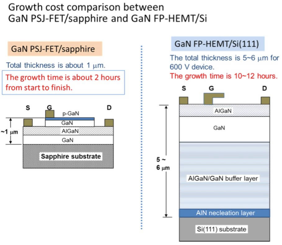
Sapphire substrate is also a common platform for GaN-LED production and the growth runs successively without chamber-cleaning. On the other hand, the growth on Si substrate needs chamber-cleaning prior to the deposition to avoid the unwanted chemical reactions between GaN and Si interface. The chamber-cleaning takes extra time and cost. As a whole, the throughput for GaN PSJ-FET/sapphire growth is roughly ten times larger than that of the GaN FP-HEMT/Si growth.

The thermal conductivity of sapphire, 40 [W/m K], is lower than that of Si, 150 [W/m K]. This problem is solved here by face-downing the die and contacting it on the base substrate, so that the heat can dissipate without going through the sapphire. As a result, the device has operated at as large as 8 amperes of the continuous current mode (CCM) under free standing (without fin) condition.


Raytheon UK’s foundry has received an order from a major fabless semiconductor manufacturer to mass produce silicon carbide (SiC) Schottky barrier diodes which are used for power conversion.

Raytheon UK’s Scottish facility will produce over 1,000 wafers in the first year. The customer will package the devices, which will have voltage ratings ranging from 600V to 1.7kV and current ratings ranging from 1 to 50A.

“This order demonstrates the increasing demand for silicon carbide semiconductors,” said John Kennedy, head of Raytheon UK’s Integrated Power Solutions.

“We have the process know-how and we’re adept at minimising the engineering costs. As an independent foundry, we have greater scope to find more innovative solutions for our customers.”

Raytheon UK’s Glenrothes foundry is the longest established independent full-scale production-qualified facility in Europe – if not the world – capable of SiC wafer processing. It has, for example, already fabricated Schottky and PiN diodes, as well as JFETs and MOSFETs, for other customers.

SiC properties include a breakdown electric field of 2,000kV/cm compared to silicon’s 300kV/cm – allowing for higher voltages; a bandgap energy of 3.26eV compared with silicon’s 1.12eV – enabling RUK007 Page 2 of 2 DECA-613 higher temperature operation; and excellent thermal conductivity (4.9W/cm.K compared with silicon’s
1.5W/cm.K).

source

X-FAB Silicon Foundries has announced it will expand the capacity and capabilities of its Kuching-based foundry operation, X-FAB Sarawak Sdn. Bhd., to meet accelerating demand for its core technologies – the 0.18µm and 0.35µm process platforms. With revenue having grown 25 percent for each of the past two years, and similar growth expected for the next two years, X-FAB plans to invest a total of US-Dollar 114 million between 2015 and 2017. This includes capex spending amounting to US-Dollar 29 million in the current year.

X-FAB Group with its clear focus on automotive, industrial and medical applications has transitioned X-FAB Sarawak from a manufacturing facility for commodity-type products into a high-value-add business for products with a long life cycle. Since it became part of the X-FAB Group in 2006, the site in Kuching has undergone a complete change in most of its technology portfolio, its application focus, its customer base, product life cycles and quality systems.

YB. Dato’ Sri Mustapa Mohamed, Minister of International Trade and Industry said, ”We are very excited that X-FAB Sarawak, one of the two pure-play semiconductor wafer foundries in Malaysia, continues to be at the forefront of our local semiconductor manufacturing industry.  The decision made by X-FAB to expand its operation in Malaysia is testament to the country’s strong economic fundamentals and the capabilities of our local talent.”

“X-FAB’s operation in Sarawak has been driving the growth of local economy. They are employing more than 1,000 staff where more than 80 percent of them are considered to be high income earners. We believe that this expansion will act as a catalyst in attracting other high technology firms to establish their operations in Malaysia as they will be able to leverage on the wafer fabrication services provided by X-FAB,” he added.

“The State of Sarawak as a major shareholder is very satisfied with the recent development of both the X-FAB Group and, more specifically, the profitable growth of X-FAB Sarawak, said Dato’ Seri Tarmizi Hj. Sulaiman, Chairman of the Board of X-FAB Silicon Foundries SE. “We are pleased that X-FAB Sarawak developed from a small nucleus into a competitive industrial enterprise with the competence and help of X-FAB.”

Rudi De Winter, CEO of X-FAB Group said, “We are looking back at nine years of successful conversion and expansion of our Sarawak foundry operation. During this period, we changed the digital business into a more future-oriented business with our complex analog/mixed-signal technologies. These technologies primarily used for automotive, industrial and medical applications enabled us to build a stable and sustainable customer base. In 2016, we expect X-FAB Sarawak for the first time to represent more than 50 percent of X-FAB Group’s total revenue.”

Mike Young, CEO of X-FAB Sarawak, added, “I am very impressed by the site’s evolution over the past several years and the success we accomplished thanks to the dedication and commitment of all our employees here at X-FAB Sarawak. Our continuous efforts to excel have paid off, as confirmed by the two awards we received in 2015 for our outstanding HR achievements, namely “The Prime Minister’s Award for Excellence in Human Resources” and “The 1Malaysia Employer Award for Big Companies.”


Source

Ascatron AB, supplier of silicon carbide (SiC) epitaxy material, and LPE SpA, a pioneer in epitaxy reactors for power electronics, have entered into a cooperation agreement to develop high performance SiC epitaxial material for volume production on 150 mm substrates. The first results demonstrating outstanding uniformity will be presented at the ICSCRM2015 conference in Catania.

Ascatron has installed a new SiC epitaxy reactor supplied by LPE in its production fab in Kista-Stockholm. The  reactor system with 150 mm wafer capability has the model name PE106. It is a new development from LPE and has recently been introduced on the market. Industry shortest cycle time and smallest footprint makes it an optimal choice for production of Ascatron’s high quality epitaxial material for high voltage power devices.

“The new production equipment from LPE is key to scale-up Ascatron advanced epitaxy processes to state-of-the-art 150 mm SiC wafers”

,says Christian Vieider, CEO of Ascatron. “We are now ready to provide our customers with n-type doped epi wafers with thicknesses from 0.1 µm up to 100 µm”.

“The new PE1O6 will further enhance Ascatron unique epitaxy based SiC technology, which is set to gain worldwide acceptance among device makers because of its superior features”, according to Franco Preti, CEO of LPE. “The cooperation with Ascatron enables LPE to strengthen our position on the market even further”.

“The single wafer concept of the LPE reactor is ideal to optimize growth parameters for a wide range of processes”, says Adolf Schöner, CTO of Ascatron.

“We are now able to establish our unique growth processes for embedded pn junctions and 3D structures on this 150 mm wafer platform, which is a crucial step towards cost effective production of next generation SiC power devices”.