– Tesla Model 3 production is ramping up, together with the production of Silicon Carbide MOSFETs used in its inverter.
– We investigated ST Microelectronics production capacity and compared it to Tesla’s production objectives.
– It look likes a shortage is slowly growing in the SiC MOSFET market, and it’s here to last.


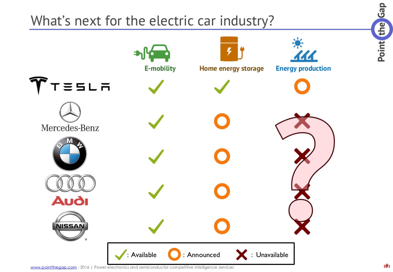
To follow the EV market, follow Tesla

Tesla has been a subject on this website and in the Power Electronics community since the first release of the Roadster and the Model S. The interest is growing as it seems the company is holding a large part of the Electric Vehicle market. They drive innovation and participate, if not define the trends. Tracking Tesla’s technology choices is tracking a big part of Electric Vehicle market technology.

The Model S was a first and very interesting Electric Vehicle. We already pointed out the special strategy of Tesla, that highly participated in the company’s success. They are not making Electric Cars for ecologic reasons, but rather make EV because it gives awesome performances to a car. They just happened to be an alternative to fossil fuel. Model S is a great example. With an almost 600 hp and a 0 to 100 km/h in 4,4 s for the “slowest” model, down to 2,4 s for the best one, It accelerates faster than Lamborghinis (yes, all of them!). But still, the Tesla Model S has 5 more seats than Lamborghinis…

The Leap: From Si IGBT Discrete to SiC MOSFET Custom Module

This first mass produced EV from Tesla has been well analyzed on our side: It uses discrete IGBTs, produced by Infineon, and we wrote a long article on the technology choices. They are using discrete components to drive the motor with a car that requires up to 1500 Amps peak. Then came Model X, the luxury SUV from Tesla. It used similar components and topologies compared to Model S, at least on the power conversion side. Tesla’s management decided to stick to what was working. It was probably a safe move to release quickly a second mass market car, and be sure to reduce production issues.

Model 3, on the other side, is expected to be the first accessible EV car with long range. It has been presented as the first “ICE” killer car (ICE: Internal Combustion Engine). For the later, Tesla’s technical team went for a completely new design. Our analysis article detailed very well the power modules, and components used (SiC MOSFET from ST Microelectronics). Tesla is already ramping up production, with more or less success. We believe they had to put some innovations on the table, and bet on the production price to drop with volume. That’s what drove them into custom made power modules with Silicon Carbide MOSFETs. No one, in the EV market, took the risk to integrate SiC at motor drive level, before Tesla and its Model 3.

Boschmann AG sintered modules - Similar to ST Microelectronics SiC modules for Tesla
Example of a AG sintered module
Similar to ST Microelectronics SiC modules for Tesla Model 3
Source: Boschmann

Investors, early buyers, competitors, suppliers and market analysts are all watching closely the Model 3 production numbers every week. PntPower is no exception to this rule. We have made our homework of analyzing Tesla’s production numbers. But one thing stroke us: How can the SiC MOSFET production follow Tesla’s needs? They reached their target of 5,000 cars produced every week by Q4-2018, each using 24 modules of 2 SiC MOSFETs. We had to compare it to ST Microelectronics production capacity.

Tesla is eating all ST Microelectronics SiC MOSFET production capacity

Following Tesla’s production is actually easy, as many investors watch closely any moves from the manufacturer (together with the SEC…). Bloomberg has a full page, auto-updated, dedicated to Tesla model 3 production status. According to that page, Model 3 is currently produced at a peak rate of about 4,500 units/week (as of Q4 2018).

Tesla Model 3 inverter, showing the SiC MOSFET power modules from ST Microelectronics

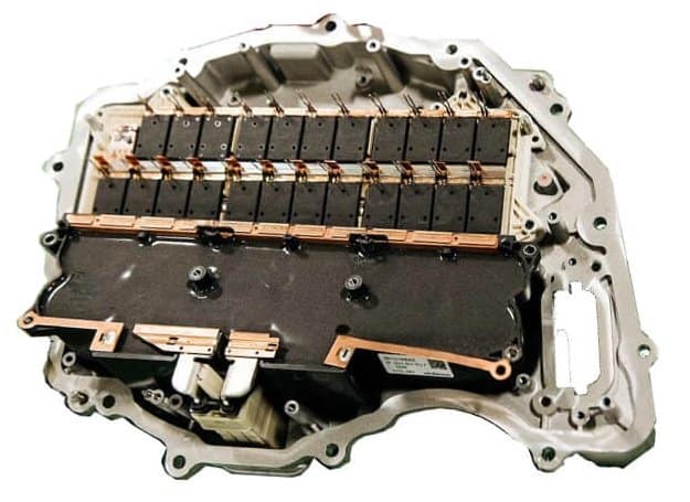
A Model 3 has one main inverter that requires 24 power modules, each of which based on two Silicon Carbide MOSFET dies. These MOSFETs are made by ST Microelectronics fab in Catania, Italy, but we will come back to it later. It is a total of 48 SiC MOSFET dies in each car.

This means Tesla need 3 Million SiC MOSFET dies every quarter to keep its production rate of Model 3, as of early January.

Now, ST Microelectronics is producing 650V/100A Silicon Carbide MOSFET from it’s fab in Catania, Italy. We took the hypothesis of a 4 mm x 4 mm die size. This matches a current density of 6.25 A/mm². They are produced on 6 inches wafers (150 mm), which is a recent fab improvement from ST Microelectronics. We believe this improvement date matches the production start for the Gen. 2 SiC MOSFET that equip Tesla electric cars. Thanks to a marvelous tool (Die Per Wafer Calculator) that every semiconductor market analyst knows very well, we can estimate the number of dies per wafer at 702. These dies are not all good, as nobody has a 100% yield, especially in manufacturing SiC MOSFET. We have to insert a bit of hypothesis here. Let say that 75% of these dies are good dies. This is already quite an optimistic figure. We based our estimation on the production capacity of ST Micro Catania: 30,000 wafers/week, including 6 in. and 8 in. production lines. The SiC line is on 6 in. wafers only. According to our sources, it’s 800 wafers/week until Q3-2018 and will ramp-up at 1000 wafers/week by Q4-2018. We estimate that 85% of this production was dedicated to Tesla in Q2 2016, in order to stock MOSFETs for Elon Musks optimistic production ramp-up back then. We known ST Microelectronics has to make some devices for other customers time to time…

Based on these numbers:

  • ST Microelectronics produced 3,420,000 SiC MOSFET modules thanks to their ramp-up
  • Tesla Model 3 production consumed 2,950,000 SiC MOSFET modules

We can easily see that, without a stock of power modules, Tesla would be quite a tight supply-chain. But mostly, Tesla’s ramp-up relies mainly on ST Microelectronics’ ramp-up, and Catania fab better be efficient, and quickly, in order to extend the reach of ST Microelectronics to other potential automotive customers

We expect ST Microelectronics and Tesla to have signed a contract during the first Model 3 design phases. They most certainly started stocking dies from the first day they knew they would need it. A main objective for them must have been to secure as much as possible. This buffer stock became their comfort mattress for any slow down in production or breach in the supply-chain. We also expect Tesla to rely partially on a second source (with a contract that might be less advantageous) to ramp-up production. This second source appears to be Infineon. But these are assumptions and even if Infineon say they are second source, we still find it difficult to integrate a different SiC MOSFET die, knowing the technology is new. A different supplier would mean driving and design tweaks.

Tesla drives the SiC MOSFET market

Summarizing all this, we do not see how Tesla’s current need for SiC MOSFET does not affect the market. There is no other way than a growing tension in supplying SiC MOSFETs to customers, and we expect it to benefit to every manufacturer in the field. Customers unable to get a SiC MOSFET from ST Microelectronics or Infineon will go to their second or third choice. It will help everyone fill their lines, and invest in larger capacity. Don’t be surprise if SiC MOSFET manufacturers smiles look more authentic than before: The power is on their side now (so to speak…).

Don’t be surprise if SiC MOSFET manufacturers smiles look more authentic than before: The power is on their side now (so to speak…).

Searching for clues

The market analysis consulting job is not only about throwing forecast about sun, rain and wind, based on assumptions from looking at the sky… We also need to evaluate the confidence we have in our estimations or hypothesis. Here we used large estimations of yield and needs, to thicken the confidence in the conclusion.

But there are other signs or clues we can follow here. A first one, is to go to a distributor website (Mouser.com, Digikey.com, Arrow.com, FutureElectronics.com). You can check for yourself, and see what is the status. At the date of publication, only one SiC MOSFET from ST Microelectronics was listed as available: 1200V/12A SCT10N120. It’s a Generation MOSFET among the first MOSFETs to be produced. We believe these stocks dates from before the Tesla-ST Microelectronics deal.


[Update 02/07/2018: We know the packaging manufacturer and added the name to the article. Devices used are  650V SiC MOSFETs and not 1200V, as stated at first. Update 09/07/2018: Packaging supply chain has been further described.]

Tesla Model 3 is using Silicon Carbide MOSFETs for its main inverter. It is now confirmed from reverse engineering analyses from different expert companies (Munro Associates and System Plus Consulting).

From Si IGBT in TO-247 to SiC MOSFETs in molded package

PntPower missed an analyst publication from August 2017 stating that ST Microelectronics was selected as a main supplier for Tesla Model 3 thanks to its SiC MOSFET at 650V. ST Microelectronics, at the time, was among the most advanced companies in SiC MOSFETs with a 1200V device already available, but nothing confirmed that SiC MOSFETs would be used as main devices for Model 3 inverter. As a reminder we extensively searched and commented the use of IGBTs in TO-247 packages in Tesla’s previous cars: Roadster, Model S and Model X. This also confirms the technological jump and the serious willingness of Tesla to become a major manufacturer of electric cars. This kind of specific design and packaging in a car is similar to the evolution of Toyota in the Prius, in a quest to improve design, density and efficiency of the HEV’s best seller, year after year.

Plastic molding and Cu ribbon-bonding: The high standard for power devices packaging

It is now confirmed that Tesla has been integrating SiC MOSFET based power modules from ST Microelectronics in Model 3 inverter. The modules are molded modules using copper ribbon-bonding for MOSFET connection. The SiC devices seems to be a 650V MOSFET at 100A made in Catania Fab (Italy), though no Automotive grade device is listed on ST Microelectronics website. The module is also very close to the most advanced technologies used today in Power Electronics packaging for automotive industry. It is to be compared with Mitsubishi electric J series TPM modules, with a cooling pad at the bottom and connections pin on the top. Packaging design has been made by a packaging expert company, based in the Netherlands, and called Advanced Packaging Center. Packaging production should be done by ST Microelectronics and/or their usual subcontractors for packaging.

Model 3 Main Inverter – Featuring 24 SiC MOSFET modules from ST Microelectronics (Source: Munro Assoc.)

1 000 000 SiC MOSFETs on the road

Tesla Model 3 manufacturing prediction from Bloomberg reach 38000 units as we speak (end of June 2018). 24 SiC MOSFET modules are used in each Model 3 inverter, this represents almost 1 Million ST Micro’s SiC MOSFETs on our roads. We will let the reader calculate the market it represents by putting its own price estimation on ST Micro’s modules.

Infineon will probably catch-up and quickly become a second source for Model 3 production in order to secure the supply-chain and follow the production ramp-up roadmap announced by Elon Musk.

Tesla made a technological jump between Model S and Model 3. It seems that Model S Power Electronic’s design objective was to quickly fulfill the power and performance requirements with off-the-shelf and available technology. On the other side, Model 3 designers might be more looking at mass-production and design and density optimization. It’s a clear sign that the Electric Vehicles market is starting to take the lead in Power Electronics innovation.

May is Sakura time and synonym of sweet weather for us in the northern hemisphere. But May is also the month when most announcements are concentrated for the Power Electronics community. It’s the month where we, at PntPower.com, have a lot of work to do.

Now that all this excitement is gone, let’s look back and have second thought about all the news and release that happened during the last weeks.

Power Module is the new SiC trend:

Some say that Silicon Carbide took too long to come. That it’s too slow and many issues still have to be solved. We have some great signs showing that it’s not dead. We can begin with Danfoss, which announced in April the opening of an assembly site on US soil, in partnership with General Electric. The move is bigger than it seems. It’s the come back of GE in the Power Semiconductor business, for the first time in a very long while. Danfoss is, for now, the exclusive user of GE’s Silicon Carbide MOSFET dies (Closed market apart: GE use their own devices).

Other Silicon Carbide MOSFET players are also more and more present and pressing:

  • Infineon announced the availability of new power modules with SiC MOSFETs. The EASY platform, well-known and widely used in a large amount of industrial and electric mobility applications, can now be ordered with SiC MOSFET.
  • Littelfuse presented its everyday growing Silicon Carbide product line. They were progressively stepping and entering the power semiconductor business, it seems now that they accelerated the process, through their partnership with Monolith Semiconductor. You will have to count on Littelfuse in the SiC Market.
  • Rohm is still growing its power module product line. The Silicon Carbide pioneer keeps going on with new products.

The slow evolution of ‘Power Electronics as a service’:

It takes some time to push an innovation and evangelize a market about a new service. That’s exactly what is happening with the power stack trend or ‘Integrated approach’.

This trend appeared a few years ago, with power components designers that wanted to offer more to their customer, in parallel with a consolidation of the market. We are talking about companies like Agile Switch in partnership with SBE capacitors and a few others or Mersen.

The trend is still here, Mersen and Agile Switch are still pushing for it, and according to them and the interview we had at PCIM, it’s starting to take off. A case study was necessary to prove how it was working. The main advantage of this trend is to be searched in the design time and lead time. You get your design done in half the time, thanks to grouped suppliers working together to assist you.

And other trends:

Gallium Nitride is still a subject but it looks like the focus has moved. We have not seen many new devices, now is the time to show how they work and what they bring. Gan power devices designers mainly showed early customers’ projects, products and all the advantages they brought.

Now is the evangelization time for GaN makers, to convince that the solution is viable and worth the investment.

The marketing of Power Electronics

Among other jobs, I have been a young (and idealist) market analysis consultant. I did my best to deliver sharp and accurate analysis and market forecasts.

There was a huge technological part in our work. Some reports were more than 200 pages with a lot of information and a lot of technology.

As a company publishing market report, we had a marketing and communications team to support us analysts. They did a great job… I can tell now that I have to take care of some of the marketing aspects of PntPower.com!

But at the time, I thought we could make much more from what we had, and I was right.

I remember seeing communication staff copy-pasting messages we passed them, to build sales and marketing material. They were literally struggling to deliver error-free material.  At each time, we were sorry to see huge mistakes in some of this material anyway. The kind of mistakes we knew was huge because technically, it did not make any sense. But how could a Corporate Communication Master’s holder see that. It’s like when you read « Gan » instead of « GaN ». It’s so easy to spot that for an engineer. It’s so easy to miss that even for a marketing rock star. I  quickly realized how much it was uneasy for non-engineers. It made me uncomfortable to have to correct them at each time.

Making more together

The young idealist I was had to started looking for a solution. I spent more and more of my time with the « Mark-com ». Most of my coffee breaks were taken on a stool in the marketing department: I was looking over the shoulder of my colleague working with me on Power Electronics and explaining what was on the screen. (Camille if you read this, do you remember these times ?)

It could be a Photoshop picture of a MOSFET :

« See, this is like a controlled switch. Gate is the control pin, and here and there are input and output. When you have voltage at Gate, you open the way to electricity flows.»

Or it could be the picture of an 8in. wafer from Infineon:

« 8in. Is the wafer size. The bigger, the more you can put devices, the cheaper the manufacturing. But it has to match with demand and production capacity… »

Weeks passed, and we all started to see less and less of these mistakes, but not only. We were also more efficient, and last but not least : The team felt stronger and better together.

That’s this last part that really made me happy of the job done.

Some missed the good in this informal teaching: It could have been interpreted as wasted time or disturbing colleagues from their initial work. But I knew I was working on a long term return for this invested time.

MOOC or SPOC: That is the Question

My secret dream when creating PntPower was to come to this. I thought that an easy accessible training, for marketing, sales, communication or any other people from your firm that are not engineers, could be an asset.

A solution is to propose on-site courses. But how much of it will trainees carry with them over time. How efficient is it, but mostly, when and how would we organize it? It’s already a nightmare to organize a conference call with everyone. Imagine the hidden cost for the firm, if we needed to gather all teams for one day, for a training day.

Online course has reached maturity and made knowledge transmission flawless. You all heard about MOOC (Massive Open Online Course). Well, when it’s not massive, we call it SPOC: Small Private Online Course.

So we took the best online course platform (OpenEdx.org) and built a course with it. It’s accessible 24/7, you can have short videos and small written sections with schematic.

The basics of Power Electronics accessible to everyone

I thought that we could and needed to explain the principles of Power Electronics without throwing Schrödinger’s equation… well… without any equation! So that’s what we did.

We built a course covering all the basics and not losing anyone in mathematics equations or semiconductor physics concepts.  It’s made of good knowledge only, useful and ready to apply – including some quiz and test.

We explained Voltage and Current through an analogy with water. We showed bands and gaps to explain what Wide Band Gap semiconductor materials. We made animations of electrons flow to show the PN Junction of the H-bridge operation.

Watch the teaser

Teaching Power Electronics to Marketing and Sales teams: is a good bet ?

Now, picture yourself in your company with all teams on the same page about Power Electronics. A new flow of ideas from marketing, new customers and opportunities from your sales teams. All the staff is able to “speak Power Electronics” and to share directly with R&D or product development.

Let’s imagine how feedback and new ideas could rain if all the different profiles of your teams could discuss and share.

The effect of a SPOC in your company

The effect of a SPOC on your teammates

I’m not talking about making your desk manager a PhD in Semiconductor physics. Just letting all the people in the company know that your R&D in Silicon Carbide might save some CO2 emissions and make the planet greener. That’s already enough. The rest will come with time, and you teaching more to them, as you just saved the time of explaining the basics and can move straight to the core topic!

Share the story to your HR, CEO or anyone in charge of training in your company. This will help your company evolve.

We know that GaN and SiC are a recurring topic, and you may be overwhelmed with it. We are sorry but what has been said about Gallium Nitride (GaN) and Silicon Carbide (SiC) power devices’ market in the past hasn’t done much good to the Power Electronics community. At PntPower.com, we want to be talk openly about what is happening. So here is our point of view.

The question is: “Who really needs GaN or SiC Power Devices?”

We’re not the kind of analyst to go through the usual message about WBG and how they are awesome and will change the world. Yes, the technology is interesting. But we strongly believe it’s not about the performances, it’s about the product/market fit. So the only question we need to ask ourselves is: What do GaN and SiC bring to power electronics systems, that IGBT, MOSFET and Super Junction MOSFET don’t?

We worked on applications-oriented market reports in order to start answering this tricky question. The idea was to define the market segments where GaN brings a real competitive advantage (not only performance-based, any competitive advantage). What we learned was: many market segments will be open to GaN penetration only when prices drop. GaN devices manufacturers may say otherwise to try and sell a wonderful world with GaN everywhere, but many applications are too cost-driven to ever be interested.

It’s quite the same story for Silicon Carbide. The technology has been here for a while, but it took time for the right product to find the right market. And that fit happened on a much higher voltage than the current product offering. So potential users had to be patient. The market estimations produced in the early days of SiC looked very optimistic for a while, now they are more reliable (only a few years later).

GaN Power Devices and SiC Power Devices’ market penetration cannot be compared

We know you had many market reports trying to tell you about this marvellous competition between the two Wide Band Gap materials, GaN and SiC. But why would GaN and SiC be in competition on the Power devices market when one gives its best at 10 kV (or so) and the other at 0.6kV (600V)? These power devices simply do not compare, and so don’t their market penetration. We cannot measure different technologies on a similar scale when they bring different advantages.

Silicon Carbide Gallium Nitride IGBT Super Junction MOSFET mapping market positionning and strategy

Extract from a Fairchild Semiconductor presentation. Designed originally by Alex AVRON, founder of PntPower.com

GaN is fit for lower voltages, high-end products. It is in direct competition with Super Junction MOSFET, when SiC is in competition with IGBT. The only voltage range SiC and GaN share could be 600V in the kilowatt range applications. But in this voltage range, we believe that GaN will quickly be cheaper than SiC, and there will be no competition. So there’s no huge fight coming up: we’re pretty sure that only one technology perfectly fits your needs.

There is a possibility that GaN reaches good performances up until 1200V later, so that’s something that could move the lines a bit in the future. But we’ll see…

Now what do the end-users and system designers feel about SiC and GaN: enthusiasts? In the end, they’re the only ones who will validate the product/market fit. The replies we had from the people we interviewed were very different from one application to another and the whole analysis is synthesized in our market report.

Teaser: the main idea is that the first market segment to adopt GaN will be the consumer applications segment.

GaN Power Devices is for Consumer markets first, and SiC will be for Transportation markets

Wide Band Gap power devices are not cheap, so the benefit of using them rather than another (cheaper) technology has to be huge. What would be that benefit, and could it be important enough to make the cost a secundary criteria? Years ago, Super Junction MOSFETs brought smaller and more efficient power supplies to consumer applications. This tendency to value size and efficiency for a device has not slowed a bit, it has even become a huge deal in the consumer market. A deal worth value, thus a deal that makes GaN interesting, despite its higher cost. Innovation is driven by high-end side.

Many have been struggling to define what the future application for Silicon Carbide MOSFET will be. The SiC material characteristics provide devices with a very high-blocking voltage (much higher than GaN, MOSFET and even IGBT). This characteristic makes it very attractive only for a limited type of application. These applications, such as rail traction or Grid and T&D, are already working on R&D development for these devices. But these segments also have very long product lifecycles (35 years for rail traction!), which makes production introduction and adoption very long.

When one technology leads to the consumer market, and the other one to complex industrial markets, we can bet that market penetration and trends will not be very similar.

The Next Steps for SiC & GaN in Power Electronics

Don’t expect Wide Band Gap to be quickly adopted in the power electronics world. Those things take time. For human reasons, for technology reasons, for money reasons. But if you want to know better what will happen for GaN in power electronics, we have a market report for that.

Curious about the SiC market? We plan on releasing an online training in 2018. Meanwhile, you can write us a message with your questions and we will give you an answer.

And the prophecy will (most likely) become true…

We (and some other blogs) wrote a lot about the laptop and consumer charger market. We tried to raise awareness and convince you that this trend is a main trend.

Although the market and supply is not going as fast as we would like it to, the market is moving.

There is activity around smaller and better laptop and smartphone chargers. As the battery market has not made the breakthrough to leave us with weeks of battery, technology relies on power electronics engineers to add to smartphones, tablets and laptops some mobility through their chargers.

Dart from Finsix, and Zolt from Avogy are now on the market, and you can buy both.


So now we know more about those two chargers that were much expected.

We have seen teardowns of the Zolt, and were (you probably were, too) disappointed to see that they used Silicon Carbide MOSFET. Problably supplied by Cree (which, in the meantime, has spinned-off its RF and Power business units, renamed the new entity Wolfspeed, the later being acquired by Infineon…).

After giving it a closer look, FinSiX Dart does not feature GaN device either. It does not even feature the VHF (30Mhz) they talked about and that the whole industry was expecting.

What does this all mean?

Delta Innergie PowerGEAR 65

Delta Innergie PowerGEAR 65


Our job is to predict the future without the use of a crystal ball (though using it is quite appealing sometimes…).

So let’s sit and think.

FinSix and the Dart

History :

  • 2010: OnChip Power was created. The objective is to built and sell power converters operating at high frequency, for the LED and lighting market.
  • 2012: OnChip Power is renamed FinSix. The company now welcomes investors and on board. Vanessa Green takes the CEO position and the strategy is redesigned from scratch. Together they define a new target: the charger market. The moto is clear, FinSix is self named worldwide leader in VHF power conversion technology (30 to 300MHz switching frequency)
  •  2014 April: FinSiX launch a product on pre-sale on a crowdfunding platform Kickstarter. It’s a laptop adapter, much smaller and convenient than comparable power adapters. They claim it wil operate at VHF (more than 30Mhz) and will revolutionize the market. +500,000USD worth of Dart products have been sold in advance of production. Initially claimed delivery date is early 2015.
  • 2016 July: Dart starts shipping to the first pre-sale customers. With more than a +18 months delay.
  • 2016 September: The first discussions on the inside of the FinSix charger, especially it’s topology, design and frequency are starting on social networks.

FinSix Dart VHF power electronics converter topology market

FinSiX Dart

It seems that Dart finally has the following characteristics :

  • Frequency of switching : 300Khz
  • External max. temperature at full load : 80°C
  • efficiency : 93.4%
  • Digital control
  • Topology : Multi-level resonant LLC half-bridge, using 4 Silicon MOSFETs

We are quite far from what we expected from FinSiX. There seems to be no GaN devices used in FinSiX charger, and there are quite far from the 30Mhz promised. On the other side, some discussions on social networks revealed a theory: maybe engineers team could not push the initial design in full production, as it’s very innovative and needs to fill in many safety regulations. So FinSiX developped a plan B, in order to have workaround and develop and alternative solution.

They delivered the product, it fits the first description and makes customer happy. It does not match the initial project design, this makes the engineers we are quite unhappy. But well, it works!


Avogy and the Zolt

Avogy is a start-up developping GaN-on-GaN power transistors. The technology is very expensive and at early stage. They created a parallel activity in which they developped a laptop charger called Zolt.

Avogy Zolt Silicon Carbide mosfet

Avogy Zolt

We already talked a lot about :

But we still expect to see different devices in future revisions of this design.

According to us, using Silicon Carbide MOSFET makes no cost sense. It shoudl be easy to replace it with GaN IC (with integrated driver, to ease the building of the new design) and cost effective. It’s quite funny for a company developping GaN-on-GaN power transistors to produce SiC chargers.

Other start-ups  :

The market is expanding now a little. Here are a few start-ups or companies in this field to watch closely :

Nordic Power Converters :

Spin-off from  DTU university, which is working on VHF converter topologies and targetting LED power supplies.

Cambridge Electronics :

Based near Boston, this start-up was created in 2012 and seems to work both at device and system level. They have presented 200V and 650V GaN devices as well as proof of concept for a power supply design.

Appulse Power :

A Start-up out from the University of Toronto, and working on digital control solutions to drastically reduce sub-100W power supplies size.

We probably missed some of the start-ups in this field. If you want us to add one, please let us know.

Conclusion:

Laptop chargers are definitely the future for power electronics innovation, especially for Wide band Gap. TSMC confirmed that by building a production line for GaN power devices and confirming the target market is laptop, smartphone and tablet chargers.

We wish it could go faster, but it looks like device makers were a bit too optimistic when they announced their products to be fully ready and on production. GaN is still a new technology to apprehend and production is not yet mastered.

But it’s coming. And we confirm our prevision of $ 370M for GaN in 2020 with a third of it for these chargers.

Foreword

News websites and market analysis companies usually do their “trends to watch this year” article in January. It’s said to help digest the turkey and resell useless X-mas presents. As Point The Power doesn’t do anything like the others, here is our “PV market trends of the year” article in September.

Introduction

Solar inverter market has always been very lively. It has grown on the basis of government subsidies and feed-in-tariffs. I agree this was necessary to launch the business. It helped cut-off the chicken and egg problem. And it’s kind of fair that our own money pays, one way or another, to build a business that’s sustainable for the planet while keeping us in our comfort.

Meanwhile, this PV business special treatment was not meant to last forever. As government decreased their help to leave the market roll by itself, rationalization came back. It was required to be more efficient, not about energy produced, but about PV inverter and PV module company’s operation. This shakes-down the market and help consolidate. We now get to a point where we will see a bit more stability.

But what to expect next.

1.500V DC input for solar farm inverter and no less!

This is the main technical trend coming and it’s strongly confirmed. Solar farm installers want higher input voltage: and 1.5kV is the most efficient one. It does not require special high voltage certification and training for installation staff, but it’s still the most efficient combination to build large multiple string installations.

Studies proved it was the best trade-off. So expect every large PV inverter manufacturer to have more and more 1500V DC input power electronics systems in their catalog very soon.

And if you are a protection or combiner box system maker I hope you are aware of that trend and ready to follow.

(Multi-)String inverter at all stages

It’s not because there is a main trend in the utility scale photovoltaic inverter field that the string inverter will stay at residential level. With prices coming down, reliability and monitoring being improved, less than 50kW string and multi-string inverters are still and will keep being used in larger installations. They will also grow in size, and you will more powerful multi-string inverter in the future.

Merger & Acquisition: A summary

The last 3 years have been very active. A lot of companies decided to leave the PV business, sell their assets,  and a few others took the opportunity to expand or enter new geographical markets.

As a picture is always more than a thousand words, take a look at our analysis here under:

Photovoltaic inverter market mergers and acquisitions solar inverter business

Integration is the leitmotiv

There has been a lot of innovation and predictions about innovation. We now feel like there is a renew, all for the best of the photovoltaic world. Tesla recently announced they are working on how to build a solar roof. They did not mean how to put solar on a roof that is already here, or integrate solar on a roof, but build a roof that produces electricity. That’s quite new in the fact that it’s targeting an unexploited market so far: People who want to renovate the roof of their house. These people could not install PV before renovation, and might not have to pay for both a roof, and then a PV installation. If both are done at the same time, the equation is changed. We believe that’s what Elon Musk see has his plan for SolarCity.

Emphase microinverter photovoltaic size reduction and power electronics integration for solar

Enphase integration power electronics size reduction photovoltaic mi

Micro inverter world is changing too. If you follow our blog, you have seen a lot of innovations in topology and use of GaN devices for Consumer and smartphone laptop chargers. These converters are a bit smaller than Microinverters but still use the same type of components (Super Junction MOSFET today, GaN Transistors tomorrow). Enphase recently confirmed that they are redesigning their product line with more integration, with faster switching for power devices and a proprietary control IC. We should see a cost reduction resulting from these innovations. This comes right when the Module Level Power Electronics (MPLE) segment is revitalized.

After Cars, Energy storage, Solar: What future for ‘Tesla Group’?

You could not have missed this last news : Tesla announced their willingness to acquire SolarCity. We already presented our analysis of a series of news from the Electric car world, where Tesla first, then several other main competitors released their plan to offer home batteries. Now Tesla is entering in the solar energy business. What’s at stake ?

Tesla is, at first, an electric car manufacturer. That’s a fact. But as a part of their strategy, they are currently building what they call their « Gigafactory ». A manufacturing site for Lithium-Ion battery able to reach up to 85GWh of packs or cells per year, by 2020. Panasonic partnered with Tesla to do so. They invested tens of billions of yen (1.5 to 3 billion USD) in the project ; which should be completed next year.

Elon Musk also revealed the Powerwall last year. It’s already available in the US. The idea is to reuse old Tesla car batteries and refurbish them to use it as a home storage system. Audi, BMW, Nissan and Mercedes-Benz now have the same plan…

Back then, when only Tesla and Mercedes-Benz had made their announcement, we released our analysis to our readers. The theory was to make a parallel between mass transportation vehicle companies and personal transportation vehicle companies. Alstom, Siemens, Bombardier, General Electric are all trains and tramway makers. Their main activity is to make transportation systems, but they also provide energy production systems through alternators or steam turbines, and also renewable energy systems. They also help transport electricity by making grid and T&D conversion systems. Just looking at the last Alstom division says it all: Alstom Transport, Alstom Grid, Alstom Energy. This happened because the core requirement to build these systems is mastering power electronics. Energy’s core competency is power electronics. So these guys, mastering Megawatt range power electronics, developed all the surrounding businesses they could.

Electric car industry moving to energy storage and production

Now let’s look closer to lower power electronics. Tesla is making electric cars, which is a small transportation system, and uses one of the core needs for that: power electronics (plus battery). They could use the same batteries and power electronics for other things: store energy at home (Tesla PowerWall), produce energy (SolarCity), propose new ways to consume energy…

That’s what is currently happening. All car makers are taking steps into storing and producing energy at home. Why car makers? They are the only ones which will produce power electronics systems at such high volumes in the future. None of the other power electronics system makers like PV inverter makers, UPS, motor drive makers or any other, can announce a production of 500,000 units/year as Elon Musk did about Tesla.

We shared this theory because we want to have your feedback about it. So share your thoughts and make us all go forward! What do you think is next for Tesla and the other car makers?

March to May is the most active period of the year for Power electronics. With the main events that are APEC and PCIM happening two months one from the other, there is a lot to do, a lot to plan and announce too. You might have been buried under tons of work and projects lately (Well, we were!). Don’t worry, PointThePower.com is here to summarize and analyze what happened, and it’s a lot!

Wide band gap field has been very active, and some other trends we announced (car maker entering the smart-grid market or the integration of intelligence in power stacks) have been a bit more confirmed.

Let’s see that in detail.

What’s new about Silicon Carbide

« Silicon Carbide is coming. » We know you have been hearing that for the last decade. So let’s pass the analysis and just go straight to the proofs:

We always said that SiC MOSFET would give its best at higher voltages. Hitachi and Mitsubishi Electric showcased their 1.7kV and 3.3kV full Silicon Carbide MOSFET. They are already filed testing these power modules on their trains in Japan. You could ride a (partially) Silicon Carbide powered trains. That is where SiC belongs, and it’s becoming real, at last.

Infineon has announced their Silicon Carbide MOSFET. It’s coming late, but it seems they did a good work. According to the presentation they gave at PCIM, they wanted to build a device that meets their requirements. They did not want to enter into a race of announcements. So the device is a Trench MOSFET – available at 1200V in samples from now, and in full production in 2017. You can basically replace chip-to-chip an IGBT with this MOSFET. It accepts the same inputs from the driver. But of course, you can get better performances using a specific power device driver. It starts sampling now but will be fully available by 2017.

Rohm also showcased a Trench SiC MOSFET, but for them it’s the third generation. The main improvement is about surge robustness which is now time higher. They recalled that they have a fully integrated supply-chain. The new devices are available at higher current (the technology was presented last year.). They now propose power modules up to 1200V/300A.

Littelfuse is investing more and more in partnership with Monolith Semiconductors to propose a full line of Silicon carbide devices and modules.

On the higher voltage side, Wolfspeed (formerly Cree power branch), Hitachi and Mitsubishi Electric make their way to higher voltages. The devices are not publicly available but tests are currently on-going. The main target for 1.7kV and 3.3kV Silicon Carbide MOSFETs are Rail traction inverters, Grid or Wind turbines.

What to expect for SiC in the next months:

We will see higher voltage devices becoming available. With wafers becoming larger (production is moving to 6 in.), we also need to expect bigger volumes of production and a reduction of production costs, thus production price. High voltage devices (1.7kV and more) will be more and more visible. It does not mean that you will be able to use them yet, but you will see more and more papers, presentations, and maybe a few public announcements about their use. R&D and design engineer will be able to put their hands on some of them, which is still very difficult today.

What’s new in GaN:

Shindengen developed and showed a Power module with GaN devices from Transphorm. Most power module maker’s start to work on the developments of their product line. They just need to « bet on the right horse ».

ViSIC is proposing sampling of its 600V GaN devices. They claim to have the best figure of merit of the market to date. Mass production will start in 2016 too. They partnered with TSMC toward this objective.

ExaGaN found a local partner to test and qualify their GaN devices.

GaN IC: a necessity?

Navitas semiconductor came out of « stealth mode ». They presented their solution which is a GaN IC. You have the GaN power device and the driver on the same die. It’s not a mixed packaged (With Silicon and Gallium Nitride, but a single die IC). It’s a 650V device processed on 6 in. wafers and samples will be available by the beginning of 2017.

Texas Instruments also released their GaN IC at 600V/12A. Even though they do not attend PCIM yet. They did not disclose much information about the device. It seems to be similar to the product develop day Navitas semiconductor having the driver integrated and thus making life easier for designers facilitate device adoption. Infineon has the same strategy with their SiC MOSFET (which is, in theory, compatible with IGBT gate drives).

What to expect for GaN in the next months

We will probably see more and more announcement, and more and more products. Some power module maker will announce the availability of their GaN based power modules. Some GaN players will have to show what they have to stay in the race (Cambridge Electronics Inc. must be working on their manufacturing process to transfer it to mass production and Powdec must be preparing their device).

Other players will make all efforts to push their devices to the market.

We have a complete analysis of the situation available in our market report « Applications and Markets for GaN in Power Electronics .» Ask us for more info.

What is left for Silicon:

Toshiba announced the fifth version of the Super Junction MOSFET. It’s based on their « Deep trench » process using deep reactive ion etching to dig a hole and build the super junction structure in it. Super Junction MOSFET is the perfect competitor to GaN today, and high-end products that use SJ MOSFET are the most likely to move to Gallium Nitride HeMT tomorrow.

Infineon showed during PCIM, a 12 in. wafer with IGBTs processed on it. They will reduce again the cost of production of IGBTs by processing them on larger wafers. It makes the target harder to reach for competition. They also showed a double sided cooled modules for hybrid and electric cars. It’s very similar to what was used in 2008 Lexus LS600h by Toyota (and developed by Denso). The module has a DBC on top and another on the bottom side.

You can also note the partnership between Nissan and Eaton, to reuse EV batteries in home storage systems. This confirms our forecast of a main supply-chain trend: similarly to Alstom, Siemens and GE in high power, electric car makers will also become part of whole ‘consumer-level’ energy complex scheme that will make Smart-grid real.

You missed your flight? Don’t worry, keep reading this page twice a day and you will have enough to make your boss think you were actually there!

You can also read this page just to know all the news, updates and gossips of Worldwide’s top Power Electronics event!

Get your load of news and updates from PCIM, Nuremberg, with our (almost) live coverage!

Last Update—Thursday 12th—Evening:

  • About GaN: Transphorm was actually there, on a booth with their local distributor. The interesting part is that they came and presented an IPM built by Shindengen with their cascode dies. It’s not a product yet but will be soon. Vincotech and all other power module makers are in the starting blocks to release their GaN based product line. The tricky being to bet on the right company.
  • About SiC: Infineon CoolSiC MOSFETs are trench MOSFETs. Infineon claimed they needed to step up to trench in order to meet their quality and performance standards.

3rd Update—Wednesday 11th—Morning:

  • About SiC: Infineon presents its SiC MOSFET (called CoolSiC) on its booth. It’s displayed on 6 inch SiC wafers.  Rohm presents the Trench SiC MOSFET. It’s their 3rd generation of Silicon Carbide MOSFET
  • About GaN: Navitas is present to talk about their monolithic GaN IC, integrating a GaN power device and its driver all on the same die.
  • About IGBT: ON Semiconductor introduced a new series of IGBTs based on their Ultra Field Trench Stop technology. These are 1200V devices in TO-247 packages, and they are already available.

2nd Update—Tuesday 10th—Evening:

1st Update—Tuesday 10th—Morning:

  • Exagan announced their partnership with Hirex engineering for test and qualification of their GaN devices, after announcing to have a fab (X-Fab) working on the production of their devices. Even though we don’t have much information about their G-FET technology, it seems that it is making its way to public availability. Wait and see, the GaN Market can be full of surprises! (By the way, Point the Power has a market report about GaN to be released this month. Drop us an e-mail to know more).
  • Littelfuse Inc. announced new SiC Schottky diodes to its portfolio of Power semiconductors. LFUSCD series now features 650V to 1200V diodes from 4A to 30A.
  • Wolfspeed announced the first All-SiC Power Module based on their MOSFET and manufactured at their Fayetteville site (formerly APEI Inc. site, acquired in 2015). It’s a 1200V/325A Half-Bridge power module.

GaN again: good news?

I remember reading a tribune on TI social blog about how much GaN discussions were exhausting these days. The author said that APEC 2015 was hammering with GaN. We have been talking about GaN over and over. And every year it’s the same thing. 2015 Rap Session at APEC concluded once more that “It’s here, it’s coming. It’s good. We need to use it.” The round-table captivated the audience, as usual, but it leads to the same talks and questions with the same kind of people. I understand it becomes exhausting. It’s too much, even for me. I would like Gallium Nitride devices to be out, used everywhere, and that we start talking about something else, like Diamond or carbon nanotubes. I wish we had passed the curve, and we were at the top of it and we were looking at something else.

But we are not there yet. We will still see a lot of GaN, but I hope and I think that we will see different GaN. Let me explain why such a theory.

Why we will see GaN again at APEC this year

We already have device start-ups and bigger companies working on Gallium Nitride devices. We know the pros and cons. We know a lot about the devices themselves. So why would we still talk about that in 2016 at APEC? I wrote recently an article about why we still cannot find GaN in small power supplies (like Zolt and maybe FinSix). GaN devices will irrigate the market in the near future. You find all the analysis, explanations and some roadmap in the GaN Market Analysis report that we’re going to release next month. But there is still a missing thing: conversion systems (and the specialists that come with it).

And Point The Gap’s belief is that this is the next step for GaN. The step where you see big companies trying to use GaN devices, and where you see a few start-ups developing new types of systems. They work on new topologies, architectures, innovative passive components, PCB design or anything needed to make GaN or SiC deliver their best. This new era has started with FinSix  back when it was still On-Chip Power and they were targeting LED power supply business. Now you also have Cambridge Electronics Inc. in Massachusetts, or Nordic Power Converter in Denmark.

You also have companies like Navitas Semiconductor, which, even though they are still in stealth mode and will probably present more during APEC, claim on their single page website that they work on GaN power ICs.

Why is Gallium Nitride good news

We all want a “GaN break ”. But it’s very good news. It means a new era is coming. Now we have companies designing systems using GaN, and innovating at conversion level. Until now, all the power conversion topologies we have developed and invented were aimed at using Silicon. It started with Silicon MOSFET, then IGBT, and Super Junction MOSFET came after that to push further the limits of Silicon. Today, the performance of Silicon has been exploited, and even if we can still improve Si devices, the gain is not as large compared to what it was 10 or 20 years ago. GaN devices are available for sampling and soon for production, and now that system designers have something to work on, I think we will watch them play with it.

Thus we will hear about GaN because we are still expecting system design (and maybe passive components design) to show us what it got.

I bet we will see a few start-up companies going out of stealth mode, and these companies won’t talk about GaN devices. They will blow our mind with GaN based conversion systems. To me, it’s a heck of a good news!

All of this will of course be included in our “GaN devices and applications in power electronics” report, to be released by April of this year.

What else than GaN ?

SiC systems (and a few devices too)

We can definitely expect more Silico-Carbide devices. We have seen and we are seeing more and more systems using SiC MOSFETs. Not much using SiC BJT or other FET. We expect this trend to keep going on. Avogy proved that we can expect GaN and finally see SiC. Maybe it will happen again. PV inverters, UPS, Air conditioning built around full-SiC power modules and discrete devices is to expect this year at APEC.

In addition to that, this is the first year Wolfspeed will attend APEC as « Wolfspeed », grouping ex-Cree Power & RF together with ex-APEI Inc. This would be a good time to announce new projects, joint work or even high-end products. APEI Inc being very good at military or Hi-rel applications.

Power stacks for high-voltage applications are mostly announced during PCIM in May in Nuremberg. I thick we will wait a few more months for these announcements.

Passive components, power stacks or new inverters ?

We will probably have some new stuff on this side. But it’s not easy to define what will be announced in which field. There are some things going-on about digital control. Integration of passive components or Power IC is also fields where we expect to see tome new things announced.

Only time will tell. PointThePower.com will attend. We will be pleased to meet with you. Drop us an e-mail and we will come to you.

Otherwise, stay tuned on the website and you will live APEC as if you traveled, there through our report to come right after the show !