Tag Archive for: Wide band gap

Ascatron signed an investment agreement with the Italian investors Quadrivio (through its venture capital fund TTVenture) and Como Venture, which now has been executed.

Quadrivio and Como Venture together received 16.7% share in Ascatron. Their aim is to continue to actively support Ascatron in order to create a leading industrial group for next generation power semiconductors based on wide bandgap material such as silicon carbide (SiC) and gallium nitride (GaN). The market is growing rapidly with an annual growth rate of 54% to reach US$ 2.0B in 2020.

“This is a first investment from international investors in Ascatron and we are very pleased to having Quadrivio and Como Venture taking lead on our current A-round fund raising”, says Christian Vieider, CEO of Ascatron.

“The money will be used to bring the Buried Grid technology for next generation high performance SiC Power electronic devices to the market”.

As part of the agreement Ascatron aquired 28.8 % of the shares in PileGrowth Tech, an Italian start-up company based in Milan. Pilegrowth has developed an innovative process for growing different semiconductor materials such as SiC on silicon. The material technology enable Ascatron to also address volume consumer markets with very competitive devices.

“The development of MOSFET transistors based on cubic SiC grown on silicon is an exciting challenge with potential to compete in the 300-1000V market with other semiconductors such as GaN”, according to Adolf Schöner, CTO of Ascatron.

About Ascatron

Ascatron develops next generation Silicon Carbide (SiC) power semiconductors radically reducing electrical conversion losses. With the 3DSiC® technology Ascatron provides the active doping structure based on epitaxy, enabling material quality and device performance unattainable through current methods. Ascatron fabricates the epitaxial material in-house and outsources processing of device wafers and chip packaging. Prototype fabrication is done in the Electrum Laboratory in Kista-Stockholm. Target applications range from high temperature for harsh environment to high voltage for wind, traction and data centers mass, as well as volume markets for solar and automotive. Ascatron started the operation in 2011 as a spin-out from the research institute Acreo, and has 10 employees in Sweden.

Hitachi Ltd and Hitachi Automotive Systems Ltd developed a high-efficiency, high-output inverter for hybrid vehicles (HEVs) and electric vehicles (EVs).

Compared with Hitachi’s existing product, the power loss of the inverter is 60% smaller, and its electric power capacity per volume is about 100% larger. The two companies expect that the new inverter will realize a long drive range and improve acceleration performance.

This time, Hitachi and Hitachi Automotive Systems developed a full-SiC power module and an inverter equipped with the module for HEVs and EVs by using SiC/GaN parallel packaging technology and double-side-cooling power module technology that they developed in the past.

SiC silicon carbide for EV HEV from Hitachi

For example, the parallel packaging technology was used to equalize the timing of switching on/off each SiC power semiconductor. In other words, a circuit board that equalizes the length of the control signal line connected to each SiC power semiconductor was developed to equalize the resistance characteristics of circuits. As a result, it became possible to fully exploit the low-resistance properties of SiC power semiconductor, increasing power capacity.

Also, for the new inverter, circuits are stacked so that the directions of load currents become opposite to one another, and it is stored in the can-like metal cooling fin of the double-side-cooling power module. As a result, the cooling fin offsets the magnetic field generated by the circuits so that the magnetic field energy stored in the circuits is reduced.

The newly-developed double-side-cooling full-SiC power module will be exhibited at the 44th Tokyo Motor Show 2015, which will be open to the public from Oct 30, 2015, in Tokyo.


Source: http://techon.nikkeibp.co.jp/atclen/news_en/15mk/092900064/

EPC corp. announce the extension of their power transistor portfolio with a high performance, wider pitch chip-scale package for ease of high volume manufacturing and enhanced compatibility with mature manufacturing processes and assembly lines.


The first in a new family of “Relaxed Pitch” devices,  the  EPC2029 80 V, 31 A eGaN  FET features a 1 mm bal l pitch.  The wider pitch allows for placement of additional and larger vias under the device to enable high current carrying capability despite the extremely small 4.6 mm x 2.6 mm footprint.

Compared to state-of-the art silicon power MOFSETs with similar on-resistance, the EPC2029 is smaller and has many times superior switching performance.  TheEPC2029 is ideal for applications such as high frequency DC-DC converters, synchronous rectification in DC/DC and AC/DC converters, motor drives, and class-D audio.

To simplify the evaluation process of this latest high performance eGaN FET, the EPC9046 development board, featuring two EPC2029 eGaN FETs in a half-bridge topology with onboard gate drive is available.  TheEPC9046 allows for easy “in circuit” performance evaluation of the EPC2029 by including all critical components and is laid out for optimal switching performance with additional area to add buck output filter components.

The new 80 V EPC2029 and corresponding development board EPC9046 are both available for immediate delivery from Digi-Key.

ON Semiconductor Corp., and Transphorm have announced a newly formed partnership to co-develop and co-market gallium nitride (GaN) based products and power system solutions for a variety of high voltage applications in the industrial, computing, telecom and networking sectors.

This strategic partnership leverages strengths inherent in both companies:

  • Transphorm is recognized as the first company to bring to market production qualified 600 volt (V) GaN on silicon transistors and has unrivalled experience working with this advanced technology.
  • ON Semiconductor is a leading supplier of energy efficient power solutions, provides significant expertise in system design, and offers an impressive portfolio that ranges from power discretes, high performance AC/DC controllers and integrated switchers to full custom ASIC power management solutions.

For power applications, GaN has been shown to deliver significant performance advantages compared to silicon based devices. The new generations of packaged products currently being co-developed by ON Semiconductor and Transphorm will provide reliable, qualified solutions that will enable designers to achieve previously unobtainable levels of efficiency and power density.

“ON Semiconductor clearly recognizes the inherent benefits that GaN technology can bring to the power electronics market and we are excited about partnering with a recognized and proven leader in this area in addition to pursuing our own GaN development work,”

said Bill Hall, executive vice president and general manager of ON Semiconductor’s Standard Products Group. “This important new collaboration strategically combines our impressive power system solution capabilities with Transphorm’s GaN expertise. Together we can bolster customer confidence in this new technology and accelerate broad market adoption.”

“Partnering with a leading power semiconductor company like ON Semiconductor reaffirms Transphorm’s GaN leadership and will provide our customers a broader set of GaN based products and solutions,” said Fumihide Esaka, CEO of Transphorm.

“This relationship is not only significant for faster penetration of GaN in the marketplace but also meaningful for the entire power conversion industry.”

The first co-developed solutions based on 600 V GaN transistors are expected to be available for sampling before the end of 2014. These solutions will address high power density applications in the 200 W to 1000 W power range for compact power supplies and adapters addressing the telecom and server markets. Under the terms of the partnership, the co-developed packaged transistor products will include low voltage MOSFET silicon from ON Semiconductor for the cascoded switch, and proven GaN high voltage High-Electron-Mobility Transistors (HEMT) from Transphorm. Co-packaging, assembly and test of the devices will be done at ON Semiconductor production facilities.

Power system reference designs will be provided to customers, enabling implementation of new solutions with GaN-based transistors and the high performance AC/DC controllers required to take full advantage of the technical benefits of GaN devices.

Source

Have you ever seen a Wide Band Gap semiconductor market report talking about laptop adaptors?

[Update 06/2016]: You want to know more about the GaN power devices market and applications? We have a market report released in June 2016, talking about that. Click here to see it!

Nobody I know and that has been working in the power electronics world, forecasted or even thought that WBG semiconductor success will come through a highly massive and common product and market as laptop chargers. They talked about power supplies and P-o-L. But they also pointed out the industrial or professional computing stuffs rather the charger in front of you right now.

Today, Laptop adaptors are massively using Super Junction MOSFET: These are MOSFETs at 600V or 900V using a specific design to enhance electron mobility (and thus efficiency and performance) beyond Silicon standards. They work, they are now massively and easily produced, they represent 61M$ market size just for laptops today and more than 900M$ over all applications. Infineon is moving product manufacturing to their brand new and bigger site in Dresden. SJ MOSFET just fit perfectly and do the job like hell. That is for today.

Zolt and finsix dart Gallium nitride based power supplies

Now let’s look at what power supplies start-ups are doing for tomorrow…

Similarly, I did not see many market reports on Wide band gap semiconductor talking about OnChip Power (former name of FINSix) and how they pivot from LED power supplies to laptop adaptors probably using Gallium Nitride power devices and high frequency conversion.

I have been following FINSix for a while, and have been curious, both professionally and personally, about their product: The Dart. It’s a real breakthrough they are working on. The same breakthrough that made transformers disappear to leave the place to Switch mode power supplies (SMPS) for portable devices. This was during the 90’s and allowed our chargers to become a little smaller, but mainly much lighter. You are not carrying hundreds of grams of a metal magnetic transformer anymore thanks to SMPS.

And FINSix is currently bringing high frequency conversion to the same public.

 We are now seeing another evolution, if not a revolution in the power adapter/charging world, that is very big for all Wide Band Gap community.

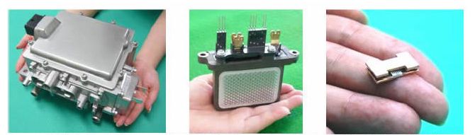
Watching Finsix make it’s way was enjoyable. I ended up learning that they were testing Transphorm GaN devices (for the most engineers among us: it’s a Cascode mounted Normally-On GaN-on-Silicon HeMT), together with an Infineon OptiMOS, to build a resonant converter. The real innovation was to transpose that topology, from military or aerospace, to mass production (Shipping has not begun yet…) for a public use.

They developed this tiny charger and managed to have enough publicity and buzz to build a company and a full business model around it. The first idea was to use the design for other purposes, but It seems that investors and deciding people thought money was somewhere else: between the wall plug and your laptop. Don’t misunderstand me: I think it’s a very good idea.

They completed a kickstarter campaign that worked very well ( almost 500,000$ and more than 4,000 pre-sales), attended several CES, and had their articles in CNet, TechCrunch, EnGadget, PCmag and a few other trendy-geeky website. They perfectly managed communication around the start-up and the product. The launch was a success; they got backed by VCs (5.2$M so far), and had media coverage.

Image capture of Finsix Dart laptop charger on kickstarter

Image capture of Finsix’s campaign on Kickstarter. See www.kickstarter.com

And you are going to ask me when is the GaN battle starting?

You don’t have a battle with a single player. And it did not take long before another GaN (Gallium Nitride) power devices manufacturer decided to build and sell their own product.

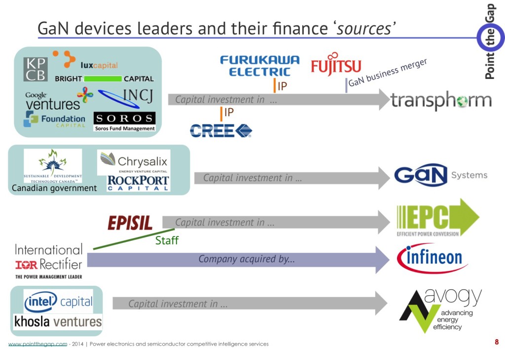
There was and there still is a battle in WBG, about which technology is best: Between GaN-on-GaN, GaN-on-Silicon or GaN-on-SiC. And the battle is still going on, with several start-up companies (GaN Systems, Transphorm, Avogy and a few others) developing and promoting their own technology.

But to win, you need to produce. You need to make your technology and your devices used in different systems. It’s the best proof that your stuff is working. And for your company to be successful, you need to sell.

Transphorm did well using that strategy. They communicated well. They managed to have their devices announced in PV inverters (with Yaskawa), motor drives, EV chargers and also these FinSix tiny laptop chargers.

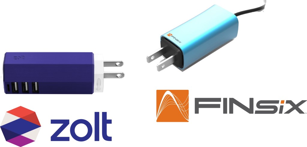
And Avogy smelled the opportunity. What happened next? They also decided to develop, announce and produce their own tiny laptop charger.

Introduced during the last CES in January 2015, the Zolt was born. It’s a bit bulkier than Finsix Dart, but with extra USB ports. It’s announced to be shipped this summer and to be in the same price range the Dart is proposed: Zolt is 79USD pre-ordered or 99USD ortherwise, Dart is 89USD pre-ordered.

And that is what I call a battle. And I say, whoever the winner is, if he manage to sell to the mass, this will be a huge market breach for Wide Band Gap semiconductor to enter in our lives (at last…).

Gan products to be released illustration: Zolt, Finsix power supplies, yaskawa pv inverter, delta ev charger and toshiba LED power supply

Extract from PointThePower.com Market report on GaN for Power electronics.

So what if Wide Band Gap semiconductor future was laptop adaptors, and nobody saw it coming?

Now, we are at a situation where FinSiX has quite a lot of pre-order from Kickstarter to be honored while the release of the product is delayed again (to this summer) and people start to complain on Kickstarter’s comments board. The Dart is even part of The Verge’s “CES 2014 products that went nowhere”

On the other side, Avogy has created a very well designed website too, and is featured in The Verge with their Zolt charger, that is announced to be ready sooner than the Dart; even though they started later (And yet there is a big battle on the marketing and communication field).

I will have a lot of questions to ask during APEC Conference in March: Meeting with Avogy and Transphorm is already planned. (NDLR: We could not meet Avogy, but we met Vanessa Green, FinSix CEO in person, and the GaN devices based version does not seem to be current version. Maybe Dart 2.0 will be? and Transphorm’s devices are not the only one being under test).

And if one of these products is a success, it will provide a maximum visibility to GaN devices, and to the company doing it.

Avogy could easily put a “Avogy GaN inside” sticker, like Rohm did for the REFU-Sol PV inverter first featured SiC MOSFETS. This is the opportunity for them to gain visibility, market shares and cash. And we all know that a combination of these three is a very good first step to success.

So let’s watch and see: Which product is released first and is a commercial success? The answer to this two question is opening the door to GaN massive adoption in power electronics.


You thought you were a geek but you did not get a thing of what is said up here? Read this:


GaN, manufacturers and devices:

Gallium nitride power devices main manufacturers and their source for founding

Extract from PointThePower.com Market report on GaN for Power electronics.

GaN is a compound material made of Gallium and Nitride. It’s a semiconductor material called Wide Band Gap. Its gap being wide provides much better performances compared to silicon, traditionally used to design semiconductor devices, even in power electronics (for electric power conversion).

But producing GaN is a complicated and expensive process. Depending on how you do it and how cheap you want it, you end having a Silicon, a SiC (another Compound semiconductor) or GaN (polycrystal) to grow monocrystal GaN on top of it, Each having their pros and cons. This will be the subject of another article.


Panasonic and Sansha Electric have announced that they have developed a compact SiC power module together with highly efficient operation of power switching systems. The SiC power module has sufficiently good reliability and greatly helps to reduce the size of power switching systems such as industrial inverters and power supplies.

The SiC power module integrates two SiC transistors into one package and achieves 6mΩ of on-state resistance with a rating current/voltage of 150A/1200V. The total volume of the module is reduced by one third compared to a conventional SiC power module. These features together with good reliability enable very compact and highly efficient power switching systems.

The developed SiC power module is based on two proprietary technologies. One is Panasonic’s SiC DioMOS (Diode-integrated MOSFET), which has the features of a reverse conducting diode without any external diode. The total chip area of SiC is reduced by half from a conventional SiC, which helps to reduce the total footprint of the module. The improved design of the DioMOS structure reduces on-state resistance to 6mΩ at 150A.

The second technology is Sansha Electric’s Techno Block module which uses solder bonding for the SiC chips without any wire bonding. This configuration reduces the height of the module by half from conventional ones as well as they can serve three times better endurance of power cycling tests.

These research and development results will be presented at the exhibition ‘The Applied Power Electrics Conference 2015’ from March 15 to 19, 2015 (Charlotte, North Carolina, US).

600V/10A GaN MISHEMT claimed to be a first for China:

Skysilicon, based in China, has released what it claims is the first GaN metal insulator semiconductor high electron mobility transistor (MISHEMT), N1BH60010A on an 8-inch GaN-on-Si wafer. This is the first 8-inch based GaN power device reported in China.

Skysilicon began the research on the GaN-on-Si power devices in July 2013. After 18 months of development, recently it successfully developed 600V/10A GaN MISHEMT on 8-inch silicon substrates, showing good switching characteristics and small parasitic capacitance.

Compared to a silicon super junction MOSFET, the GaN MISHEMT can reduce parasitic capacitance up to 90 percent says Skysilicon. The GaN research program in Skysilicon is funded by Chinese National Science and Technology Major Project (NSTMP), aiming to develop 8-inch based GaN-on-Si power devices and technologies.

Skysilicon is a semiconductor device manufacturer focused on power electronics. The main products of Skysilicon are discrete power device and power IC, MEMS sensors and compound semiconductor devices. The company built the GaN-on-Si power device platform on its own 8-inch manufactory line, which is suitable for high volume production.

More info here

Toshiba Lighting & Technology Corp developed a halogen lamp-shaped LED light bulb using a GaN (gallium nitride) power device for its power supply circuit.

The LED lamp will be released March 6, 2015. With the GaN power device, it can be operated with a frequency of 700kHz, which is about 10 times higher than the operating frequency of the company’s previous product using a Si (silicon) power device. As a result, the area of the new LED lamp’s main power supply circuit is about 40% that of the previous product’s main power supply circuit.

A dimming function was added by using the saved space. With a chip for phase-control dimming and software for controlling dimming, the “Premium Dimming Technology” of the new lamp supports not only dimmers dedicated to LED lamps but also dimmers for incandescent light bulbs. The technology reduces flickering caused by the fluctuation of power supply voltage and waveform distortion. In addition, it enables to smoothly adjust light intensity from 0% (extinction) to 100%.

Toshiba Lighting & Technology will release two models whose light fluxes are 200lm and 250lm, respectively. The manufacturer’s suggested retail prices of them are both ¥7,500 (approx US$62.2, excluding tax). The company aims to sell 60,000 units of the two models combined.

It plans to exhibit the new product at Lighting Fair 2015, which runs from March 3 to 6, 2015, in Tokyo.

Source

Raytheon UK is lending its expertise in high-temperature silicon carbide (HiTSiC) to partner on a project that would provide aircraft electronics and wiring with a device to protect against lightning strikes.

The innovative project – led by Controls and Data Services (part of the Rolls-Royce Group) and which also includes Newcastle University in the role of design authority and TT Electronics Semelab – is exploring the use of Raytheon’s and Newcastle University’s HiTSic technology to make Current Limiting Diodes (CLDs); a new kind of lightning protection device which stands to reduce the amount of electrical energy traditional suppressors have to deal with during a lightning strike.

“With today’s composite materials replacing metallic components and skin materials, the reduced electrical screening in airframes is forcing a rethink of lightning protection architectures,” said John Kennedy, head of Raytheon UK’s Integrated Power Solutions.

“Current Limiting Diodes will essentially absorb much of the electrical energy that the dampening device would otherwise have to channel during a lightning strike.”

The two-phase project, funded under Innovate UK, is currently in phase one; Newcastle University is conducting electrical characterization tests while TT Electronics Semelab develops the CLD packaging.

With the project expected to be completed by late 2015, Raytheon UK’s innovative high-temperature silicon carbide solution to guard against lightning strikes will soon be the eye in the storm.

More info here


1. Who is this “Rohm” again…?

Kyoto based Rohm Semiconductor is the technology leader of SiC power devices. They have been the first to release SiC Schottky diodes, SiC MOSFET in 2010 and Full-SiC power modules in 2012.

They also master the full supply chain since the acquisition of the German SiC wafer manufacturer SiCrystal in 2009. They have access to German made 6-inch wafers since 2013.

According to their roadmap, showed and diffused during conferences in 2014, they are currently working on their 3rd Generation of SiC MOSFET to be released soon.

rohm roadmap on SiC diodes and mosfet releasing generation in 2015 and going up to 1700V

They will use a Trench Gate, together with a Trench Source. This Trench Source will allow reduction of the electric field and thus highly improve performances of SiC MOSFETS.

Roadmaps planned the release of these devices for 2015, and as APEC conference in Charlotte is approaching, the question has been raised.

Rohm kyoto based second generation and third generation of SiC mosfet. planar gate versus trench gate mosfet

Rohm 2nd and 3rd generation of SiC Mosfet

Will APEC be the day when Rohm will make a new step in the Wide band gap power electronics world by releasing its own SiC 1700V switch?

2. A bit of technology:

The 1700V breakdown voltage is very important in Japan. This is the voltage limit where devices can easily be used in Rail traction. You know how rail traction is important in Japan, in terms of sales but also in terms of image. If Rohm is able to gain market shares in auxiliary rail traction converters and light rail in Japan, they will have another advantage over the biggest European semiconductor companies.

They are working on 17A and 50A bare dies.

The 650V and 1200V devices will also adopt the new 3rd Generation U-MOS design, based on trenches.

3. And a tiny bit about competition:

As a reminder, Rohm is already supplying many system makers in Europe, with SiC devices for R&D and advanced design.

Cree is doing a good job too. But we believe that power is not their main target. Cash is coming from LED for them and power electronics is just extra-money.

And you can also note that their communication is getting better as well. They were already doing good products. Now, if they manage to sell them well, they can quickly become a very big competitor for the IGBT dinosaurs!


Sumitomo Chemical has agreed today with Hitachi Metals, Ltd. to acquire their compound semiconductor materials business. The acquisition is due to take place, effective April 1, 2015.

The business that Sumitomo Chemical will acquire from Hitachi Metals includes those of compound semiconductor materials, such as gallium nitride (GaN) substrates, GaN epiwafers, and gallium arsenide (GaAs) epiwafers. As far as GaN substrates and epiwafers are concerned, Hitachi Metals is a forerunner in the field and boasts its state-of-the-art technology.


The acquisition will allow Sumitomo Chemical to expand its business of GaN substrates and epiwafers for use in electronic and optical components, for which the market is taking off on a full scale, while at the same time devoting its efforts to early commercialization of the products for use in power devices.

Source

Point the Power’s insight:

Sumitomo is a huge Japanese group. Chemicals are not their only activity in electronics. SEI, their electric division is actively using compound semiconductors. They developed Silicon Carbide MOSFET technology that has been released in 2013 and it is not a surprise if they are also actively working on Gallium Nitride devices. Their product portfolio goes far beyond power electronics. They are active in all electronics, connectors, materials applications as well.

The new SCT20N120 silicon-carbide power MOSFET from STMicroelectronics brings advanced efficiency and reliability to a broader range of energy-conscious applications such as inverters for electric/hybrid vehicles, solar or wind power generation, high-efficiency drives, power supplies, and smart-grid equipment.

SiC Silicon carbide ST microelectronics MOSFET 1200V device power electronics semiconductor

ST is among the few vendors leading the development of the robust and efficient silicon-carbide power semiconductors. The 1200V SCT20N120 extends the family, with on-resistance (RDS(ON)) better than 290mΩ all the way to the 200°C maximum operating junction temperature. Switching performance is also consistent over temperature thanks to highly stable turn-off energy (Eoff) and gate charge (Qg). The resulting low conduction and switching losses, combined with ultra-low leakage current, simplify thermal management and maximize reliability.

In addition to their lower energy losses, ST’s SiC MOSFET permit switching frequencies up to three times higher than similar-rated silicon IGBTs allow. This enables designers to specify smaller external components and save size, weight, and bill-of-materials costs. The SCT20N120’s high-temperature capability helps to simplify cooling-system design in applications such as power modules for electric vehicles.

The SCT20N120 comes with the added advantage of ST’s proprietary HiP247™ package with enhanced thermal efficiency, which allows reliable operation up to 200°C while maintaining compatibility with the industry-standard TO-247 power-package outline.

For further information please visit: http://www.st.com/sicmos

Our point of view:

ST Microelectronics is part of the few SiC MOSFET manufacturers. The leader in this field being the Kyoto-Japan based manufacturer Rohm. There are other players who preferred another technology (JFET, Bipolar) but the specific designs that they require does not make them great competitors. Today, MOSFET is the most used device.

1200V is the right voltage where Silicon Carbide material starts to give its potential. Applications as Renewable energies, Heavy industrial applications are among the targets. They represent a very good sales volume versus average price trade-off.