Tag Archive for: Device

Flosfia Inc and a research group of Kyoto University succeeded in making a p-type layer necessary for realizing an “gallium oxide” (Ga2O3)-based power transistor.

Flosfia is a venture firm based in Kyoto, Japan, and the research group is led by Shizuo Fujita and Kentaro Kaneko, professor and assistant professor, respectively, of the Graduate School of Engineering and Faculty of Engineering, Kyoto University.

Gallium oxide is drawing attention as a material that potentially enables to make a power device with a higher withstand voltage, lower loss and lower cost than SiC (silicon carbide) and GaN (gallium nitride), which are being developed as the next-generation power semiconductor materials.

This time, the researchers used the “α-type” gallium oxide, which has a crystalline structure called “corundum.” They realized the p-type layer by using iridium oxide (Ir2O3), which has the same corundum structure as the α-type gallium oxide, making it possible to form a gallium oxide-based power MOSFET.

N- and p-type layers are necessary for realizing a power MOSFET, and it has been very difficult to make a high-quality p-type layer by using gallium oxide.

This time, Flosfia and the research group focused on iridium oxide. It has the same corundum structure as the α-type gallium oxide, and the difference in lattice constant between them is as small as 0.3%. And the researchers consider that it is possible to make a power MOSFET by using n-type gallium oxide and p-type iridium oxide. Flosfia aims to ship samples of a gallium oxide-based MOSFET in 2018.

Flosfia makes the “α-type” gallium oxide by using the “Mist Epitaxy” method. And the same method can be applied to iridium oxide, the company said. The method was developed by combining the company’s own technologies such as a technology to reduce impurity concentration and a multi-layer technology based on the “Mist CVD” method developed by Fujita and others. The Mist Epitaxy method eliminates the need for expensive vacuum devices.

The p-type characteristics of iridium oxide were confirmed by hall effect measurement. Its hall mobility and carrier concentration were 2.3cm2/Vs and 1.0 x 10²¹/cm3, respectively. Its corundum structure was confirmed by X-ray diffraction profile and diffraction spot.

Source

Wolfspeed, a Cree Company and a silicon carbide (SiC) power devices, power modules and system maker, has introduced a 1000V MOSFET.

SiC MOSFET  Specifications:
The new 1000V, 65mOhm MOSFET is available in a through-hole, 4L-TO247 package and is listed as part number C3M0065100K and is currently available for purchase at Digikey, Mouser and Richardson RFPD. Wolfspeed plans to release another 1000V MOSFET in a 4L-TO247 package at 120mOhm (C3M0120100K) in the coming weeks. This package has a Kelvin-source connection that allows engineers to create designs that maximize the benefits of SiC’s superior speed and efficiency.

The surface-mount versions of these devices, C3M0065100J and C3M0120100J, will be released later this year. Like the 4L-TO247, the surface mount devices include a Kelvin-source pin to help minimize gate-ringing and reduce system losses.

Target markets and applications:

“Supporting the widespread implementation of off-board charging stations, Wolfspeed’s technology enables smaller, more efficient charging systems that provide higher power charging at lower overall cost. This market requires high efficiency and wide output voltage range to address the various electric vehicle battery voltages being introduced by automotive suppliers,”

explained John Palmour, CTO of Wolfspeed.

“Wolfspeed’s new 1000V SiC MOSFET offers system designers ultra-fast switching speeds with a fraction of a silicon MOSFET’s switching losses. The figure-of-merit delivered by this device is beyond the reach of any competing silicon-based MOSFET,” Palmour added.

Source

VisIC Technologies, Ltd. Is announcing the launch of a new product, offered in a smaller package with bottom side cooling, an on resistance (RDS(ON)) rating of 0.080Ω, and a reduced external components requirement using a simplified driving scheme.

This new 650V GaN Power Switch is a member of the ALL-Switch family designed for bridge converters in motor drives, power supplies, chargers, UPS, Inverters and other circuits requiring high efficiency and currents up to 12A.

VisIC Technology’s designs operate with lower gate charge and capacitance than competitive products while providing the benefits of low RDS(ON). Offered in low inductance packaging, the ALL-Switch family is able to deliver high efficiency. For comparison, ALL-Switch’s switching losses are 3-5 times lower than comparable SIC MOSFET transistors operating at the same frequency.

The V80N65B answers the need expressed by many of VisIC’s customers for a bottom- side cooled package in their designs after they have experienced ALL-Switch’s low switching losses.

The V80N65B Bottom-side cooled power switch supplements VisIC’s, existing ALL Switch top-side cooled product line of 650V GaN devices: The V22N65A, V22S65A, and V18G65A.

ON Semiconductor Corporation announced today that the U.S. Federal Trade Commission has accepted a proposed consent order for public comment and has terminated the Hart-Scott-Rodino waiting period applicable to ON Semiconductor’s proposed acquisition of Fairchild Semiconductor International, Inc. Under the proposed consent order and in order to satisfy the FTC’s remaining concerns, prior to the closing of the acquisition of Fairchild, the FTC required that ON Semiconductor dispose of its planar insulated gate bipolar transistor (“Ignition IGBT”) business, which business generated less than $25 million in revenue during fiscal year 2015. In satisfaction of this requirement, ON Semiconductor announced today that it has entered into a definitive agreement with respect to the divestiture of the Ignition IGBT business to Littelfuse, Inc. and has also entered into a separate definitive agreement with Littelfuse to sell its transient voltage suppression (“TVS”) diode and switching thyristor product lines, for a combined $104 million in cash. No manufacturing assets will be transferred by ON Semiconductor in connection with the divestiture of the Ignition IGBT business or the sale of the TVS and thyristor businesses, and both asset sales are expected to close on August 29, 2016.

ON Semiconductor acquisitions conditions Fairchild Littelfuse

The completion of ON Semiconductor’s previously announced tender offer (the “Offer”) to purchase all of the outstanding shares of common stock of Fairchild for $20.00 per share in cash remains subject to certain customary terms and conditions set forth in the Offer to Purchase, dated December 4, 2015, as amended (the “Offer to Purchase”), and other related materials by which the Offer is being made.

The condition to the Offer relating to the termination or expiration of required waiting periods under the HSR Act has been satisfied. The proposed FTC consent order is subject to public comment for 30 days and to final approval by the FTC, although this will not affect the parties’ ability to close the transaction when all other conditions to closing have been satisfied.

Dialog Semiconductor, a provider of power management, AC/DC power conversion, solid state lighting (SSL) and Bluetooth® low energy technology, today announced and is demonstrating its first gallium nitride (GaN) power IC product offering, using Taiwan Semiconductor Manufacturing Corporation’s (TSMCs) 650 Volt GaN-on-Silicon process technology.

The DA8801 together with Dialog’s patented digital Rapid Charge™ power conversion controllers will enable more efficient, smaller, and higher power density adapters compared to traditional Silicon field-effect transistor (FET) based designs today. Dialog is initially targeting the fast charging smartphone and computing adapter segment with its GaN solutions, where it already enjoys more than 70 percent market share with its power conversion controllers.

“The exceptional performance of GaN transistors allows customers to deliver more efficient and compact power adapter designs that meet today’s market demands,”

said Mark Tyndall, SVP Corporate Development and Strategy, Dialog Semiconductor. “Following our success in BCD-based power management ICs (PMICs), as an early GaN innovator, Dialog once again leads the commercialization of a new power technology into high-volume consumer applications.”

GaN technology offers the world’s fastest transistors, which are the core of high-frequency and ultra-efficient power conversion. Dialog’s DA8801 half-bridge integrates building blocks, such as gate drives and level shifting circuits, with 650V power switches to deliver an optimized solution that reduces power losses by up to 50 percent, with up to 94 percent power efficiency. The product allows for a seamless implementation of GaN, avoiding complex circuitry, needed to drive discrete GaN power switches.

The new technology allows a reduction in the size of power electronics by up to 50 percent, enabling a typical 45 Watt adapter design today to fit into a 25 Watt or smaller form factor. This reduction in size will enable true universal chargers for mobile devices.

“As Dialog’s strategic foundry partner for power management ICs for many years, we are delighted to have expanded our relationship to collaborate closely in bringing our GaN process to the mainstream consumer market for high volume applications,” said Maria Marced, President of TSMC Europe. “Dialog’s first GaN product delivers on the promise of GaN while bringing the integration to a higher level.”

The DA8801 will be available in sample quantities in Q4 2016. More information on the DA8801 can be found here:  http://www.dialog-semiconductor.com/products/DA8801

Watch the DA8801 GaN video here: https://youtu.be/O9ks-j0R6PA

Source

Mitsubishi Electric Corporation  announced today the launch of a new transfer-mold power semiconductor model in its lineup of Super-mini Dual-In-line Package Intelligent Power Modules (DIPIPMTM), embedded with Silicon Carbide Metal-Oxide-Semiconductor Field-Effect Transistors (SiC-MOSFET). It will launch on August 17.

Product Features

1) Top class low power consumption in the home appliance market

SiC-MOSFET reduces power consumption by about 70 percent compared with Mitsubishi Electric’s existing Super-mini DIPIPM, and contributes to an overall reduction in air conditioner power consumption
2) Simplified inverter system design

Footprint and pin configurations are compatible with Mitsubishi Electric’s existing Super mini DIPIPM Ver.6, PSSxxS92x6series,etc.
Designed with a high threshold voltage, SiC-MOSFET does not require a negative bias circuit, allowing simplification of the system design
Fewer external components due to use of embedded bootstrap diode with current-limiting resistor

Sales Schedule

Model Specification Shipment
PSF15S92F6 15A/600V August 17, 2016

source

STMicroelectronics has introduced a portfolio of TO-220 FullPAK (TO-220FP) wide creepage power transistors, including the world’s first 1500V super-junction MOSFET in this new important arcing-resistant package.STMicroelectronics Introduces New Super-Junction MOSFETs including World’s First 1500V Device in TO-220FP Wide Creepage Package

The TO-220FP wide creepage package is ideal for the power transistors of open-frame power supplies commonly used in equipment such as television sets and PCs, which are vulnerable to surface contamination by dust and particles that can cause high-voltage arcing between transistor terminals. The new package’s extended lead spacing of 4.25mm eliminates the special potting, lead forming, sleeving, or sealing needed to prevent the arcing when using conventional packages with 2.54mm lead spacing. Power-supply manufacturers can now meet applicable safety standards and minimize field failures without applying these additional processes, thereby simplifying manufacturing and enhancing productivity.

While providing superior arcing resistance, TO-220FP wide creepage retains the outstanding electrical properties of the popular TO-220FP. Moreover, similar outer dimensions help streamline design-in and ensure compatibility with established assembly processes.

ST developed the TO-220FP wide creepage package by collaborating with its customer SoluM, a leading power manufacturer based in Korea. SoluM is using the superior package to create new power solutions that are more robust and cost-effective than competing products.

ST is currently ramping up production of TO-220FP wide creepage power transistors to support a major global television manufacturer. The product portfolio includes four fully qualified 600V low-RDS(ON) MDmesh™ M2 MOSFETs with current ratings from 8A to 34A. The 1500V STFH12N150K5 and 1200V STFH12N120K5, MDmesh K5 devices, will be qualified by the end of Q3 2016.

Toyoda Gosei Co., Ltd. has developed the world’s first 1.2 kV class power semiconductor device (a general term for power rectifier diodes, switching transistors, etc.) chip capable of large current operation exceeding 20 A. This was done using gallium nitride (GaN), a key material in blue LEDs, which has superior physical properties including the ability to withstand high voltages.

Toyoda gosei GaN 1.2kV hemt power electronics

Using the crystal growth technology we have cultivated since 1986 in the development and production of blue LEDs, we began research for the development of device technology for power semiconductors using GaN in 2010. Previously, low loss MOSFETs (a type of transistor used in power devices*) of the 1.2 kV class were fabricated on GaN substrates and then empirically tested. We have now established wiring technology for the parallel operation of elements, successfully passing an electrical current exceeding 20 A in a vertical GaN transistor with a 1.5 mm square chip size. This is the first time that has ever been achieved, according to a Toyoda Gosei survey.

The developed technology are applied to circuits for the power controllers on hybrid vehicles that handle large amounts of power, and to power converters such as those in solar power generation, which promises significant contributions in making these devices more compact and efficient. We will continue research to increase the current capacity and test reliability with the aim of developing commercial applications by about 2018-2020 in collaboration with semiconductor and electronics manufacturers.

Source

ROHM has recently announced the availability of a new 1700V SiC MOSFET optimized for industrial applications, including manufacturing equipment and high-voltage general-purpose inverters.

In recent years, the growing trend to conserve energy in all areas has increased the demand for energy-saving power semiconductors, particularly for applications in the industrial sector such as general-purpose inverters and manufacturing equipment. In the majority of auxiliary power supplies, which are used to provide drive voltages for power supply circuits, control ICs, and various supplementary systems, high breakdown (1000V+) silicon MOSFETs are normally utilized. However, these high-voltage MOSFETs suffer from large conduction loss (often leading to excessive heat generation), and present problems related to mounting area and the number of external components, making it difficult to reduce system size. In response, ROHM developed low-loss SiC MOSFETs and control ICs that maximize performance while contributing to end-product miniaturization.

Rohm-sic-boardgraph

The SCT2H12NZ provides the high breakdown voltage required for auxiliary power supplies in industrial equipment. Conduction loss is reduced by 8x over conventional silicon MOSFETs, contributing to greater energy efficiency. And combining with ROHM’s AC/DC converter control IC designed specifically for SiC MOSFET drive (BD7682FJ-LB) will make it possible to maximize performance and improve efficiency by up to 6%. This allows smaller peripheral components to be used, leading to increased miniaturization.

1. Optimized for auxiliary power supplies in industrial equipment
Compared to 1500V silicon MOSFETs used in auxiliary power supplies for industrial equipment, the SCT2H12NZ provides higher breakdown voltage (1700V) with 8x smaller ON resistance (1.15Ω). In addition, the compact TO-3PFM package maintains the creepage distance (distance measured along the surface of the insulating material) required by industrial equipment. ROHM is releasing a surface mount type (TO268-2L) that also provides adequate creepage distance.

2. Improved efficiency when combined with ROHM’s dedicated IC
Using this latest SiC MOSFET in combination with ROHM’s AC/DC converter control IC (BD7682FJ-LB) designed specifically for SiC MOSFET drive will make it possible to maximize performance and increase efficiency by up to 6%. At the same time heat generation will be reduced, minimizing thermal countermeasures and enabling the use of smaller components.

3. Simply evaluation by using ROHM’s evaluation board for SiC devices
As a comprehensive semiconductor manufacturer, ROHM offers a broad lineup of ICs optimized for use with a variety of SiC devices. ROHM is also launching evaluation boards and kits that make it possible to immediately begin evaluation and development. In addition to the BD7682FJ-LB-EVK-402, a gate drive board for evaluating ROHM’s full SiC module along with a snubber module are offered. More information can be found on ROHM’s dedicated support page.

Applications
Auxiliary power supplies for high voltage (i.e. 400VAC) industrial equipment such as factory automation (robots), solar and industrial inverters, and manufacturing/testing devices

Part Number Package Polarity VDSS ID PD
(Tc=25ºC)
RDS(on)
VGS=18V
QG
VGS=18V
NEW SCT2H12NZ TO-3PFM Nch 1700V 3.7A 35W 1.15Ω(typ.) 14nC (typ.)
Under Development SCT2H12NY TO-268-2L
(Surface Mount)
4A 44W
Under Development SCT2750NY 5.9A 57W 0.75Ω(typ.) 17nC (typ.)

 Sic MOSFET 2

TT Electronics today launched a Silicon Carbide (SiC) power MOSFET that is designed for high temperature, power efficiency applications with a maximum junction temperature of +225°C. As a result of this operating potential, the package has a higher ambient temperature capability and can therefore be used in applications, including distribution control systems with greater environmental challenges, such as those in close proximity to a combustion engine.

Supplied in a high power dissipation, low thermal resistance, fully hermetic, ceramic SMD1 package the 25A, 650V rated SML25SCM650N2B also ensures faster switching and low switching losses in comparison to normal Si type MOSFETs, consequently the size of the passive components in the circuit can be reduced resulting in weight and space saving benefits. The N-channel MOSFET features a total power dissipation of 90W at a TJ temperature of 25 degrees. A range of screening options are available.

For use in applications that require faster switching in high temperature power conversion topologies and systems, the SML25SCM650N2B will find favour with design engineers working in industrial power conversion applications including oil drilling, distributed management control systems, renewable energy applications / power conversion, space systems and applications.

Silicon Carbide is the new semiconductor technology of choice to help power electronic design engineers design with more efficiency, with higher operating temperatures to lay the foundation for future conversion and control system design demands. With the SML25SCM650N2B, the combination of new Silicon Carbide technology with a high reliability, industry standard outline hermetic packaging technology coupled with TT Electronics’ renowned Lutterworth based design and manufacturing capability delivers value and very high performance to the end customer.

source

VisIC Technologies is pleased to announce availability of its new generation of ALL-Switch V22S65A (with an internal SiC diode) and V22N65A (without internal SiC diode).

This new version of VisIC’s ALL-Switch significantly reduces the MILLER effect enabling readily available, standard drivers to be used in VisIC-based designs. These new devices also reduce the bill of materials required for specific applications.

Extremely effective in hard switching topologies, the V22 series may be used for Zero Voltage Switching or Zero Current Switching topologies. It has the lowest Rdson among either 650V GaN or SiC MOSFET transistors, and can achieve extremely efficient power conversion with slew rate exceeding 100V/nS.

In addition, since the threshold voltage exceeds 5V, the devices work well in harsh EMI environments.

VisIC Technologies has demonstrated worldwide record   with performance of its Half Bridge demonstration board, achieving better than 99.3 % peak efficiency at 200 kHz in a hard-switched topology providing 2.5KW output.

VisIC allswitch GaN device with integrated SiC diode

About VisIC Technologies Ltd

Based in Nes Ziona, Israel, VisIC Technologies, Ltd. was established in 2010 by experts in Gallium Nitride (GaN) technology to develop and sell advanced GaN-based power conversion products.  VisIC has successfully developed, and is bringing to market, high power GaN-based transistors and modules.  (GaN is expected to replace most of the Silicon-based (Si) products currently used in power conversion systems.) VisIC has been granted keystone patents for GaN technology and has additional patents pending.

For more information please access our website: http://www.visic-tech.com . The highest efficiency with GaN.

For additional information, please contact:
Eli Zenouda – Director Sales & Marketing
+972-54-2296641
eliz@visic-tech.com

Source

March to May is the most active period of the year for Power electronics. With the main events that are APEC and PCIM happening two months one from the other, there is a lot to do, a lot to plan and announce too. You might have been buried under tons of work and projects lately (Well, we were!). Don’t worry, PointThePower.com is here to summarize and analyze what happened, and it’s a lot!

Wide band gap field has been very active, and some other trends we announced (car maker entering the smart-grid market or the integration of intelligence in power stacks) have been a bit more confirmed.

Let’s see that in detail.

What’s new about Silicon Carbide

« Silicon Carbide is coming. » We know you have been hearing that for the last decade. So let’s pass the analysis and just go straight to the proofs:

We always said that SiC MOSFET would give its best at higher voltages. Hitachi and Mitsubishi Electric showcased their 1.7kV and 3.3kV full Silicon Carbide MOSFET. They are already filed testing these power modules on their trains in Japan. You could ride a (partially) Silicon Carbide powered trains. That is where SiC belongs, and it’s becoming real, at last.

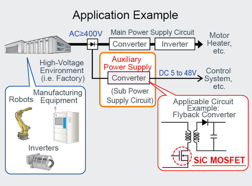
Infineon has announced their Silicon Carbide MOSFET. It’s coming late, but it seems they did a good work. According to the presentation they gave at PCIM, they wanted to build a device that meets their requirements. They did not want to enter into a race of announcements. So the device is a Trench MOSFET – available at 1200V in samples from now, and in full production in 2017. You can basically replace chip-to-chip an IGBT with this MOSFET. It accepts the same inputs from the driver. But of course, you can get better performances using a specific power device driver. It starts sampling now but will be fully available by 2017.

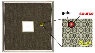
Rohm also showcased a Trench SiC MOSFET, but for them it’s the third generation. The main improvement is about surge robustness which is now time higher. They recalled that they have a fully integrated supply-chain. The new devices are available at higher current (the technology was presented last year.). They now propose power modules up to 1200V/300A.

Littelfuse is investing more and more in partnership with Monolith Semiconductors to propose a full line of Silicon carbide devices and modules.

On the higher voltage side, Wolfspeed (formerly Cree power branch), Hitachi and Mitsubishi Electric make their way to higher voltages. The devices are not publicly available but tests are currently on-going. The main target for 1.7kV and 3.3kV Silicon Carbide MOSFETs are Rail traction inverters, Grid or Wind turbines.

What to expect for SiC in the next months:

We will see higher voltage devices becoming available. With wafers becoming larger (production is moving to 6 in.), we also need to expect bigger volumes of production and a reduction of production costs, thus production price. High voltage devices (1.7kV and more) will be more and more visible. It does not mean that you will be able to use them yet, but you will see more and more papers, presentations, and maybe a few public announcements about their use. R&D and design engineer will be able to put their hands on some of them, which is still very difficult today.

What’s new in GaN:

Shindengen developed and showed a Power module with GaN devices from Transphorm. Most power module maker’s start to work on the developments of their product line. They just need to « bet on the right horse ».

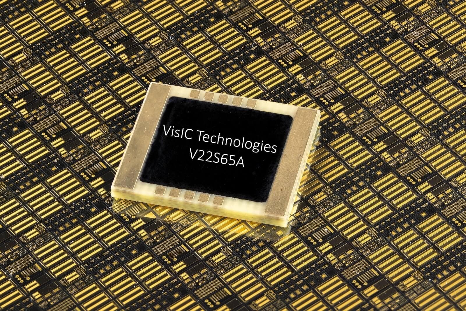
ViSIC is proposing sampling of its 600V GaN devices. They claim to have the best figure of merit of the market to date. Mass production will start in 2016 too. They partnered with TSMC toward this objective.

ExaGaN found a local partner to test and qualify their GaN devices.

GaN IC: a necessity?

Navitas semiconductor came out of « stealth mode ». They presented their solution which is a GaN IC. You have the GaN power device and the driver on the same die. It’s not a mixed packaged (With Silicon and Gallium Nitride, but a single die IC). It’s a 650V device processed on 6 in. wafers and samples will be available by the beginning of 2017.

Texas Instruments also released their GaN IC at 600V/12A. Even though they do not attend PCIM yet. They did not disclose much information about the device. It seems to be similar to the product develop day Navitas semiconductor having the driver integrated and thus making life easier for designers facilitate device adoption. Infineon has the same strategy with their SiC MOSFET (which is, in theory, compatible with IGBT gate drives).

What to expect for GaN in the next months

We will probably see more and more announcement, and more and more products. Some power module maker will announce the availability of their GaN based power modules. Some GaN players will have to show what they have to stay in the race (Cambridge Electronics Inc. must be working on their manufacturing process to transfer it to mass production and Powdec must be preparing their device).

Other players will make all efforts to push their devices to the market.

We have a complete analysis of the situation available in our market report « Applications and Markets for GaN in Power Electronics .» Ask us for more info.

What is left for Silicon:

Toshiba announced the fifth version of the Super Junction MOSFET. It’s based on their « Deep trench » process using deep reactive ion etching to dig a hole and build the super junction structure in it. Super Junction MOSFET is the perfect competitor to GaN today, and high-end products that use SJ MOSFET are the most likely to move to Gallium Nitride HeMT tomorrow.

Infineon showed during PCIM, a 12 in. wafer with IGBTs processed on it. They will reduce again the cost of production of IGBTs by processing them on larger wafers. It makes the target harder to reach for competition. They also showed a double sided cooled modules for hybrid and electric cars. It’s very similar to what was used in 2008 Lexus LS600h by Toyota (and developed by Denso). The module has a DBC on top and another on the bottom side.

You can also note the partnership between Nissan and Eaton, to reuse EV batteries in home storage systems. This confirms our forecast of a main supply-chain trend: similarly to Alstom, Siemens and GE in high power, electric car makers will also become part of whole ‘consumer-level’ energy complex scheme that will make Smart-grid real.