
Powdec prepares 1.2kV GaN/Sapphire transistors for 2017

POWDEC has succeeded in making GaN PSJ (Polarized Super Junction) transistors on sapphire substrate having both 1,200 V rating-voltage and the on-resistance of less than 100 mΩ.
Powdec has developed a PSJ (Polarization Super-junction) structure instead of the FP (Field-Plate). The PSJ is so strong against the current collapse that sapphire can be used as substrate. As a result, the device is free from the electric breakdown caused by the substrate. And Powdec succeeded in obtaining up to 6 kV of the breakdown voltage for the device with GaN thickness as thin as 1 μm.
GaN-on-Si devices are applied to the conversion systems only below 600 V rating range. However, the present achievements using the unique PSJ-on-sapphire platform shows that the PSJ devices can enter into the application fields where Si-IGBTs dominate today.
What is Polarized Super Junction?
SJ (Super-junction) is a structure to improve both the conductivity and the breakdown voltage of the Si power-MOS transistor. The drift layer consists of thin p/n stacks while the conventional one consists of a single n-type layer. PSJ (Polarization Super-junction) is a method to implement the SJ effect in the GaN/AlGaN system where the polarization effect functions as SJ.
GaN-on-Silicon versus GaN-on-Sapphire:
Most GaN device makers develop GaN-on-Silicon (or GaN/Si) power devices. Powdec’s 1,200V devices are GaN-on-Sapphire devices. Not using the Silicon and using Sapphire implies intrinsic differences in the device structure and operation.
GaN-on-Si power devices:
GaN power devices today are implemented on Si(111) substrate, which is called “GaN-on-Si” or “GaN/Si”. The thickness of the nitride layers needed for 600V rating devices is generally 5μm or more. The GaN/Si devices are equipped with Field-plates (FP are conductive plates set on the gate to split the steep electric field). FPs are indivisibly needed for the conductive Si substrate to mitigate the current collapses. Current-collapse is another name for the current decreasing phenomenon during the transistor operation. The channel electrons are scattered and deployed around the channel by the strong electric field. These immobile electrons act as the negative bias for the channel resulting in the decrease of the current.
Advantages of GaN-on-Sapphire for Power devices:
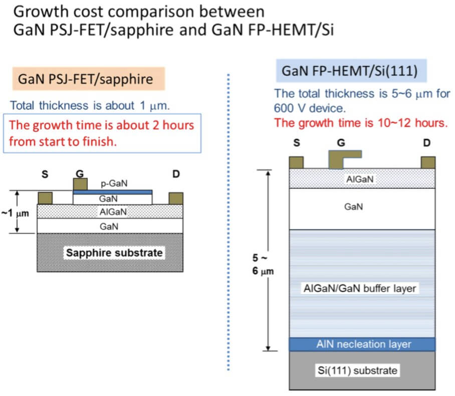 Sapphire substrate is also a common platform for GaN-LED production and the growth runs successively without chamber-cleaning. On the other hand, the growth on Si substrate needs chamber-cleaning prior to the deposition to avoid the unwanted chemical reactions between GaN and Si interface. The chamber-cleaning takes extra time and cost. As a whole, the throughput for GaN PSJ-FET/sapphire growth is roughly ten times larger than that of the GaN FP-HEMT/Si growth.
The thermal conductivity of sapphire, 40 [W/m K], is lower than that of Si, 150 [W/m K]. This problem is solved here by face-downing the die and contacting it on the base substrate, so that the heat can dissipate without going through the sapphire. As a result, the device has operated at as large as 8 amperes of the continuous current mode (CCM) under free standing (without fin) condition.


Leave a Reply
Want to join the discussion?Feel free to contribute!