Tag Archive for: SiC

CISSOID, the leader in high-temperature and extended lifetime semiconductor solutions, announces the delivery of the first prototypes of a 3-phase 1200V/100A SiC MOSFET Intelligent Power Modules (IPM) to Thales Avionics Electrical Systems. This module, developed with the support of Clean Sky Joint Undertaking, will help increasing power converters density, by decreasing weight and size, for power generation and electromechanical actuators in More-Electrical Aircrafts.

This IPM offers an optimal integration of the gate driver with power transistors together in order to take advantage of the full benefits of Silicon Carbide (SiC), i.e. low switching losses and high operating temperature. Leveraging on HADES2® Isolated Gate Driver that incorporates years of development in driving SiC transistors, it combines advanced packaging technologies enabling a reliable operation of power modules in extreme conditions.

For this Aerospace module, a 3-phase power inverter topology was selected while other topologies are being investigated for HEV and Railways projects. In this 3-phase topology, each of the 6 switch positions includes a 100A SiC MOSFET transistor and a 100A SiC Schottky free-wheeling diode. These devices can block voltages up to 1200V, which provide enough headroom against over-voltages in a 540V Aerospace DC bus, and the module is designed to be easily upgraded with 1700V/150A SiC devices. The transistors have a typical On resistance of 12.5mOhms or 8.5mOhms depending on their current rating, either 100A or 150A.

CISSOID SiC power module Avionics more electric aircraft

Special care was put on thermal aspects during the design of the module. First, all the materials have been selected to allow reliable operation at high junction temperatures, up to 200°C with peaks at 225°C, in order to decrease cooling requirements. This materials selection also enables high case and storage temperatures, up to 150°C. Finally, the module is based on high-performance materials such as AlSiC baseplate, AlN substrates and Silver Sintering in order to offer near perfect CTE matching with SiC devices and high robustness against thermal and power cycling.

Co-designing the gate driver with the power module in a single IPM allowed CISSOID to optimize the gate driver circuit taking into account parasitic inductances of the power module while minimizing them when possible. Minimizing parasitic inductances allows to switch SiC transistors faster and to lower switching losses. An IPM also offers a plug-and-play solution to power electronic designers who save a lot of time in the design of the gate driver board, which is particulary challenging with SiC transistors. They can then focus on the design of high density power converters taking advantage of SiC.

“It was a pleasure to work with CISSOID team in the frame of this Clean Sky program. They showed a great flexibility in proposing us solutions addressing the requirements of the next generation of high density power converters for the More-Electrical-Aircraft”

said Taoufik Bensalah, Power Converter Design Team Manager at Thales Avionics. Etienne Vanzieleghem, VP Engineering at CISSOID added: “We are very glad with this fruitful cooperation with Thales and with the open discussions we had in specifying this IPM. We also thank Clean Sky for making this cooperation possible which is a good example of CISSOID combined expertise in packaging and circuit design. This project was also an opportunity to strengthen our cooperation with PRIMES platform in Tarbes which is hosting CISSOID packaging team.”

Source

X-FAB Silicon Foundries of Erfurt, Germany – a mixed-signal IC, sensor and micro-electro-mechanical systems (MEMS) foundry – has entered wide-bandgap semiconductor production by announcing the availability of silicon carbide (SiC) foundry from its wafer fabrication plant in Lubbock, Texas.

The firm says that, due to major internal investments in the conversion of capital equipment (as well as the support provided by the PowerAmerica Institute at North Carolina State University), X-FAB Texas has heavily upgraded its manufacturing resources in order to be ‘SiC-ready’. Among the tools now added are a high-temperature anneal furnace, backgrind equipment for thinning SiC wafers, backside metal sputter and backside laser anneal tools. A high-temperature implanter is scheduled for installation later this year. X-FAB can hence now fully leverage the economies of scale that are already available in its established 30,000 wafer per month silicon line, presenting the market with the means to produce large volumes of SiC devices on 6-inch wafers.

X- FAB says that, as well as its 6-inch wafer capabilities, other key differentiators include higher yields and accelerated ramp-up to full-scale production, plus decades of experience in manufacturing semiconductor devices that adhere to the most stringent quality standards (such as those for automotive applications). The firm will not only supply fabless semiconductor vendors but also act as a second source for integrated device manufacturers (IDMs) with their own SiC production capabilities.

“Current SiC offerings are either IDMs creating their own products or relatively small foundry operations using 4-inch production facilities,” says Andy Wilson, X-FAB’s director of strategic business development. “X-FAB is bringing something different to the market, with a SiC capacity of 5000 wafers/month ready to utilize and potential to raise this further,” he adds. “We can thus offer a scalable, high-quality, secure platform that will enable customers to cost-effectively obtain discrete devices on SiC substrates and also safely apply vital differentiation.”

In 2015, SiC diode and MOSFET supplier Monolith Semiconductor Inc of Ithaca, NY, USA relocated its headquarters from Ithaca, New York, to Round Rock, Texas, following a strategic partnership announced in 2014 for the manufacture of its SiC switches in X-FAB Texas’ high-volume 150mm silicon production line.

Source

Fairchild has released its first 1200V SiC diode, the FFSH40120ADN. The company says the diode’s combination of superior switching performance, higher reliability and low electromagnetic interference (EMI) make it suitable for next-generation solar inverters, industrial motor controls and welders.

“The combination of market trends and tightening industry standards is driving the need for more energy efficient products and our new 1200V SiC diode is designed specifically to help manufacturers achieve these ever-greater efficiency requirements and with better reliability, ruggedness and cost efficiency,”

said Jin Zhao, VP and general manager of Fairchild’s High Power Industrial division.

“We based this diode on SiC due to the material’s considerable advantages over silicon, and we will add additional SiC-based semiconductors as we build a comprehensive family of SiC solutions,” he added.

The FFSH40120ADN diode is claimed to have the best leakage current performance in its class, leaking far less current than its competitors at temperatures up to 175degC. Other benefits of the new diode include fast switching and no reverse recovery current, which reduces switching losses compared to silicon and results in superior energy efficiency.

The diode’s ability to switch stably over a wide temperature range is another factor contributing to its performance, as is its zero recovery voltage which eliminates voltage overshoots.

Fairchild will demonstrate the performance of the new diode at the upcoming APEC conference, March 20-24 in Long Beach, California.

Source

X-FAB Silicon Foundries is putting itself at the vanguard of wide-bandgap semiconductor production by announcing the availability of its silicon carbide (SiC) offering from its wafer fab in Lubbock, Texas.

Thanks to major internal investments in the conversion of capital equipment, as well as the support provided by the PowerAmerica Institute at NC State University, X-FAB Texas has heavily upgraded its manufacturing resources in order to make them “SiC-ready”. Among the tools now added are a high-temperature anneal furnace, backgrind equipment for thinning SiC wafers, backside metal sputter and backside laser anneal tools. A high-temperature implanter is scheduled for installation later this year. X-FAB can, as a result, now fully leverage the economies of scale that are already available in its established 30K wafer per month silicon line, thereby presenting the market with the means to produce large volumes of SiC devices on 6-inch wafers.

As well as X-FAB’s 6-inch wafer capabilities, other key differentiators need to be factored into the SiC equation. Among these will be higher yields and accelerated ramp-up to full scale production, plus the company’s decades of experience in manufacturing semiconductor devices which adhere to the most stringent quality standards, such as those for automotive applications. Not only will X-FAB supply fabless semiconductor vendors, the company will also be well positioned to serve as a second source solution for IDMs with their own SiC manufacturing.

“Current SiC offerings are either IDMs creating their own products or relatively small foundry operations using 4-inch production facilities,” states Andy Wilson, X-FAB’s Director of Strategic Business Development. “X-FAB is bringing something different to the market, with a SiC capacity of 5k wafers/month ready to utilize and potential to raise this further. We can thus offer a scalable, high quality, secure platform that will enable customers to cost-effectively obtain discrete devices on SiC substrates and also safely apply vital differentiation.”

Source

Basic 3C Inc., a Longmont startup aiming to go to market soon with a new type of semiconductor, has added about $650,000 from existing investors to a Series A round of funding.

Basic 3C president Bart Van Zeghbroeck said this week that the hope is that the latest funds get the company through the next six months before raising a Series B.

Founded in April 2014, the company — based at 1830 Boston Ave. — has been in product-development mode, but is hoping to commercialize its first product in the next six months.

Basic 3C’s semiconductors will be made from cubic silicon carbide, rather than silicon. Geared toward high-power applications operating at 600 volts or more that require efficient power conversion, the product will have higher thermal conductivity and do well in “operationally rugged environments,” Van Zeghbroeck said. He said targeted applications include solar panels, wind turbines and electric vehicles. A reduced cooling requirement would mean reduced size and weight and thus, in something like an electric vehicle, improved efficiency and range.

“We’re looking at significantly better material properties, and that makes a difference in the end application,” Van Zeghbroeck said.

Investors in the company include Boulder-based Infield Capital and Texas-based Dankat LLC.

Van Zeghbroeck is on leave from the University of Colorado, where he has been an electrical engineering professor since 1990. He and investors purchased the technology and intellectual property for Basic 3C from a Golden company, Silicon Carbide Systems, that had gone bankrupt.

Van Zeghbroeck said Basic 3C will initially do manufacturing at its current space in Longmont. The company has fewer than 10 employees, but he said he expects that number to grow to 15 or 20 within the next 18 months.

Sanken Electric has expanded its lineup of SiC Schottky diodes. The new FMDA-10565 SiC Schottky is rated for 650V and 5A with a typical forward voltage drop of 1.5V at 25°C. Taking advantage of the high speed switching capability of SiC, these diodes achieve reduced switching loss, and reduced reverse leakage current at high temperatures. At 25°C, typical leakage current is 15 µA at a junction temperature of 150°C, typical leakage current is 70 µA.

he FMDA-10565 is designed for use in PFC sections, motor drive circuits and inverters in applications such as servers, communications power equipment, air conditioners, and so on. Packaged in a TO220F-2L, these Schottky’s have a temperature coefficient of 2.5°C/W and an operating junction temperature range of -40 to 175°C.

These devices are particularly well-suited for continuous current mode PFC circuits. They are capable of reducing the power loss that results from the recovery current. The diode’s high-speed switching capability and energy-saving functionality allows for the potential downsizing of equipment. The 5A FMDA-10565 is the third device in this family and it joins the 10A FMCA-11065 and the 20A FMCA-22065.

[Update 23/02/2016: We had several questions and feedback about this article. We would like to specify its context, hypothesis and boundaries. As specified in the title, this analysis is focusing on a specific application at a given time. We are talking about small laptop chargers for a design made during 2014 with a product released during 2015. This analysis is to change as fast as technologies, manufacturability and product availability will change. We would be happy to have your point of view as well. Please comment if you agree or disagree!]

Our last blog post about GaN in laptop chargers has been widely spread, read and appreciated (even in the French magazine electroniques.biz). On the other side it left some hypothesis, particularly on the type of devices used in these new FinSix Dart and Avogy Zolt laptop chargers. There was no information at the time. Device makers claimed they were suppliers but nothing could confirm it.

Zolt contains a SiC MOSFET from Cree:

Avogy Zolt laptop charger SiC device
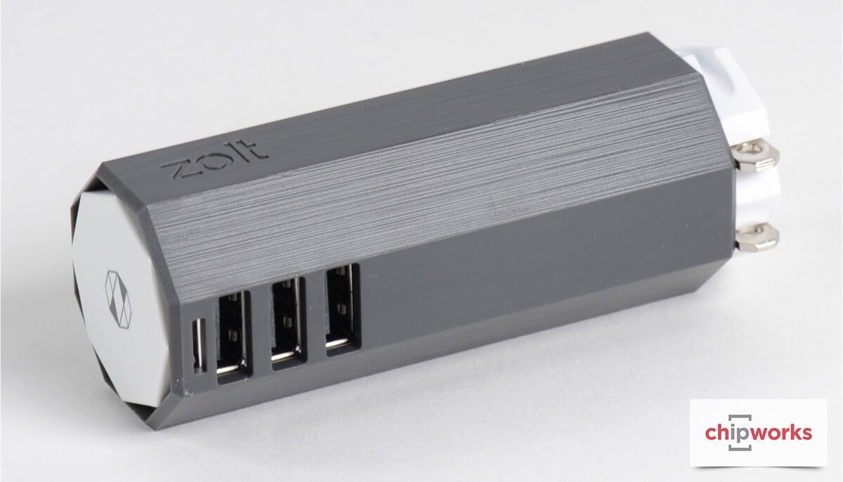
We do have one Zolt charger at PointThePower.com but we don’t have the lab to tear it down… Our friends from Chipworks did a very well job dismantling and revealing the inside of Zolt.  It was a striking news : Zolt contains an Avogy power device with a Cree1 Silicon Carbide MOSFET (repackaged by Avogy).

We were sure that GaN was the best device for this application, not SiC. And we are still sure about that. We thought that FINsix and Avogy managed to design their laptop charger using Super-Junction MOSFETs and fast smaller MOSFETs. It appears they did not. What option is left then? Silicon Carbide MOSFET.

But if you step back…

There are a few reasons that would lead one to go to SiC rather GaN, for now:

  1. Don’t trust GaN device makers: 600V is not available for production volumes!

Here are two examples to prove my word:

  • I recently read back interviews with two famous GaN makers stating 600V devices will be available by late 2014. We’re in 2016 now and the same makers do not have it yet.
  • I received an e-mail from a reader last year, pointing at a GaN power device announced in January. It disappeared from the catalog in May. We have no news since then.

I’m sure you all have similar examples in mind. So even if the GaN power device market says it’s ready, I want proofs that devices are available for this specific application. We will investigate these proofs in a market report to be released in April this year. We also have GaN devices teardown reports from our LTEC Corp., Our partner.

  1. Silicon Carbide MOSFET is expensive, but available and working

Chipworks Zolt Laptop charger SiC Cree mosfet

Chipworks’ picture of Zolt Laptop charger with SiC MOSFET

Avogy could order SiC MOSFETs and package them as flip-chip SMD. It seems devices switching faster than SJ-MOSFET was something required for their charger design. This is something possible with Silicon carbide if you are willing to pay the price. It’s a bit more difficult using GaN, even if you are in a wealthy company reading to lose some money.

  1. You don’t need the best charger, you need a working tinier charger… fast!

Have you seen FINSix Kickstarter campaign? I don’t blame them, I’m sure they did the work at its best and I know unexpected issues always rise in an engineering project. But similarly to other crowdfunding campaigns, they are late in the delivery of their Dart chargers. That makes backers a bit mad. Avogy managed to deliver less late compared to FINSix. They also designed something quite fast to make it available. This is a winning strategy that required to pick available devices: Silicon Carbide was the preferred solution.

Image capture of Finsix Dart laptop charger on kickstarter

Image capture of Finsix’s campaign on Kickstarter. See www.kickstarter.com

  1. LED and laptop charger market is about size: not efficiency, not lifetime, and not even price!

Yes: not even price. The chargers that we are talking about are expensive. A Zolt is 99 USD, Dart is about the same price. You have to add an extra 20 bucks if you own an Apple laptop. That is more expensive than Apple chargers, which are the most expensive laptop chargers on the market.

So, for a third-party charger this is very expensive. And with these 10 extra bucks you can definitely put a few dollars in a SiC device rather than struggling with a Super-Junction MOSFET. A third option would be to go for GaN, which will probably be cheaper than SiC when it’s available. We did miss that in our analysis of the situation.

There is also no need for a long lifetime as it’s targeting consumer electronics. These products have a maximum life of 3 to 5 years. Why would the charger last more?

Conclusion: SiC vs. GaN leaves SiC as a winner…in 2015

Again it’s all about availability. SiC has been around for 15 years. Gallium Nitride is much newer. So expecting GaN to be ready yet as SiC is still struggling to establish is quite optimistic. GaN will be ready and as of the characteristics we see, we expect it to eat a great amount of the market shares from Super Junction MOSFET. You get can get more information by downloading the sample of our market report: We will establish how, when and where is this market report to be published in April.

GaN-devices

Extract from PointThePower.com Market report to be released April 2016 – (c) Point The Gap

Combine all these reasons together and the best shot if you were designing a small charger using LLC resonant converter topology is either to go for Super Junction MOSFET and optimize cooling like hell… or put one SiC MOSFET die to ease your cooling and optimization design, and be sure you have devices to manufacture you chargers.

I have been working as a market analyst for a few years now, and I start to know about the market, about market players and their habits. There is a common habit in power devices market and start-up world: They are often optimistic.

PointThePower.com tries not to spread too much optimism: because it leads to disappointment.

Notes:

1: Cree has spin-off its RF and Power business units and merged it with APEI Inc, a company they acquired recently. The new entity is called Wolfspeed.


Gruppo PBM, a leader in industrial battery chargers, is using SiC MOSFETs in its new HF9 battery charger family to enable higher efficiency and power density at a lower overall system cost.

Demand for safe, efficient and fast-charging industrial batteries has increased exponentially along with the proliferation of power electronics. The HF9 product family is designed to provide the highest possible efficiency while achieving easy scalability for power ranging from six to 16 kilowatts. These benefits are made possible in part by Wolfspeed 1200V SiC MOSFET technology.

“We selected Wolfspeed SiC Planar MOSFETs for our new HF9 battery charger family because they enabled us to improve our battery chargers while achieving operational savings, increased productivity and increased safety. This was not possible with the best IGBTs in the market,”

said both Marco Mazzanti and Giancarlo Ceo, who respectively serve as CTO and R&D Engineer at Gruppo PBM.

Based in Italy, Gruppo PBM specializes in rugged high-frequency battery chargers, dischargers and testers. By using Wolfspeed SiC MOSFETs in its latest HF9 family, Gruppo PBM not only achieves improved efficiency, but also a reduction in component count, improving the overall reliability in the system by lowering the operating temperatures and—most importantly—reducing overall system cost.

“Wolfspeed’s SiC MOSFETs, especially our new C3M 900V family, are enjoying rapid adoption in the growing battery charger market segment,” explained Edgar Ayerbe, Wolfspeed’s power MOSFET marketing manager. “Our products increase power density and dramatically lower switching losses, making it possible to introduce smaller, cooler and lower cost chargers for the automotive and industrial markets.”

Sourcehttp://www.wolfspeed.com/news/gruppo-pbm

As part of the company’s strategy to move more significantly into power semiconductors for industrial and automotive markets, Littelfuse has made an investment in Monolith Semiconductor, Inc., a start-up company developing silicon carbide technology. Silicon carbide is a rapidly emerging semiconductor material that enables power devices to operate at higher switching frequencies and temperatures versus conventional silicon. This allows inverters and other energy conversion systems to be built with significantly improved power density, energy efficiency and cost.

“Investing in and partnering with Monolith’s experienced team of silicon carbide and power semiconductor experts allows us to quickly evolve our portfolio with strategically relevant and innovative technology,”

said Ian Highley, Littelfuse Senior VP and GM, Semiconductor Products, and CTO.

“Silicon carbide power technology is among the most promising advancements in the semiconductor market today. It will be an important tool in helping us solve complex problems for our customers.”

“Forming this strategic partnership with Littelfuse accelerates development and helps bring silicon carbide technology to the market,” said Sujit Banerjee, PhD, CEO of Monolith Semiconductor. “Littelfuse is an ideal partner for us. We are excited to dramatically increase our customer reach, gain access to global channels, and benefit from their sales and marketing depth and expertise.”

Initially this is not a material investment for Littelfuse; however, the company has committed to add to its investment once Monolith has achieved certain milestones. This investment is not expected to have any material financial impact on Littelfuse in 2015 or 2016.

About Littelfuse
Founded in 1927, Littelfuse is the world leader in protection with growing global platforms in power controls and sensing. The company serves global customers in the electronics, automotive and industrial markets with technologies including fuses, semiconductors, polymers, ceramics, relays and sensors. Littelfuse has over 8,000 employees in more than 35 locations throughout the Americas, Europe and Asia. For more information, please visit the Littelfuse website: Littelfuse.com.

About Monolith Semiconductor
Monolith Semiconductor Inc., a Round Rock, Texas-based startup company, is focused on improving the affordability and reliability of SiC power devices by utilizing advanced manufacturing techniques and high-performance processes and designs. For more information, please visit the Monolith Semiconductor website: monolithsemi.com.

Source

Raytheon UK’s foundry has received an order from a major fabless semiconductor manufacturer to mass produce silicon carbide (SiC) Schottky barrier diodes which are used for power conversion.

Raytheon UK’s Scottish facility will produce over 1,000 wafers in the first year. The customer will package the devices, which will have voltage ratings ranging from 600V to 1.7kV and current ratings ranging from 1 to 50A.

“This order demonstrates the increasing demand for silicon carbide semiconductors,” said John Kennedy, head of Raytheon UK’s Integrated Power Solutions.

“We have the process know-how and we’re adept at minimising the engineering costs. As an independent foundry, we have greater scope to find more innovative solutions for our customers.”

Raytheon UK’s Glenrothes foundry is the longest established independent full-scale production-qualified facility in Europe – if not the world – capable of SiC wafer processing. It has, for example, already fabricated Schottky and PiN diodes, as well as JFETs and MOSFETs, for other customers.

SiC properties include a breakdown electric field of 2,000kV/cm compared to silicon’s 300kV/cm – allowing for higher voltages; a bandgap energy of 3.26eV compared with silicon’s 1.12eV – enabling RUK007 Page 2 of 2 DECA-613 higher temperature operation; and excellent thermal conductivity (4.9W/cm.K compared with silicon’s
1.5W/cm.K).

source

Wolfspeed, the new spin-off from Cree, that makes silicon carbide (SiC) and gallium nitride (GaN) wide-bandgap semiconductor devices, has launched what it claims is the industry’s first 1700V SiC MOSFET offered in an optimized surface-mount (SMD) package. The higher blocking voltage enables design engineers to replace lower-rated silicon MOSFETs with the new SiC MOSFETs, delivering higher efficiency, simplified driver circuitry, and lower thermal dissipation, and resulting in lower total system costs, says the firm.

The new SMD package, specifically designed for high-voltage MOSFETs, has a small footprint with a wide creepage distance (7mm between drain and source). This is made possible by the small die size and high blocking capability of Wolfspeed’s SiC planar MOS technology. The new package also includes a separate driver source connection, which reduces gate ringing and provides clean gate signals.

“Our new 1700V SiC MOSFET provides power electronics engineers with significant design advantages, particularly in flyback topologies,”

claims Edgar Ayerbe, marketing manager for power MOSFETs. “Due to the lower switching losses of silicon carbide, the devices operate at much lower junction temperatures. This enables customers to directly mount the devices onto the PCB with no additional heat-sinks, which greatly reduces the manufacturing costs and improves the reliability of the systems,” he adds.

“The result is a smaller, lighter power supply with a lower system cost than is possible using silicon devices.”

Application of the new 1700V SiC MOSFET is anticipated in auxiliary power supplies within high-power inverters — such as solar power inverters, motor drives, uninterruptible power system (UPS) equipment, wind-energy converters, and traction power systems — which typically buck down DC voltages to operate system logic, protection circuitry, displays, network interface, and cooling fans. They can also be used in the power supplies of three-phase e-meters, or in any converter application that requires high blocking voltages and low capacitance.

Designated the C2M1000170J, the new 1700V SiC MOSFET features an avalanche rating greater than 1800V, and an RDS(on) on-resistance of 1Ω. These characteristics ensure reliable performance in flyback converter circuits, including those in noisy electrical environments such as those found in high-power inverters, says Wolfspeed. By enabling the design of single-switch flyback topologies from input voltages spanning 200V to 1000V, the 1700V SiC MOSFET simplifies the complex drive and snubber circuit elements required for silicon devices, the firm adds.

The C2M1000170J is fully qualified and available for sampling now.