
Fujitsu puts GaN in high efficiency 12-W AC adapter

Fujitsu Laboratories Ltd. today announced the development of the world’s smallest, most efficient AC adapter, which uses gallium nitride (GaN) high electron-mobility transistor (HEMT) power devices for super-fast charging of smartphones and other mobile electronics.
Note: This news is totally in line with what Point The Power announced in its insight article in June. A market report is currently under edition: more info here.
As mobile devices using AC adapters to recharge such as smartphones, tablets, and other electronics powered by rechargeable batteries have become more and more prevalent, charger efficiency has become an issue in reducing the total amount of power consumed and reducing society’s environmental footprint. As mobile devices are built with increasing battery capacity, charging those batteries quickly becomes an issue, creating a demand for compact, high-output AC adapters.
Fujitsu Laboratories has now used low dynamic resistance GaN-HEMT as the switching element, which is heavily by low-loss, to develop the world’s smallest and most efficient AC adapter. New circuitry that precisely controls switching timing reduces current loss, allowing for the world’s smallest 12-W AC adapter (15.6-cc) and the world’s most efficient power supply at 87%. Using GaN-HEMPT has made it possible to have small, high-speed switching as well as achieve low-resistance and improved energy efficiency. With this technology, AC adapters charging mobile electronics will consume half the power and will be able to charge in one-third of the time. Widespread use of this AC adapter will help reduce CO2 emissions and reduce burden on the environment.
The prototype AC adapter will be exhibited at Eco-Products 2015, from December 10 at Tokyo Big Sight.
Background
The has been an rapid increase in prevalence of cellphones, smartphones, tablets, and other mobile electronics powered by rechargeable batteries and there are pressing needs for high-capacity battery-equipped mobile electronics with long run times, and to charge such devices quickly, making smaller and higher-output AC adapters even more desirable. In addressing their environmental impact, reducing power consumption has become an issue. In February 2016, the U.S. Department of Energy will be putting into effect revised “Level-VI” efficiency standards for external power supplies, calling for power supplies operating at 6-V or less to increase their efficiency by as much as 5.46%. Meeting this higher efficiency level has been a significant undertaking.
Issues
AC adapters today use a switching-based approach with field-effect transistors (FET) as the switching elements, which repeatedly turn on and off to convert and thereby control the voltage.
The most effective means of improving the size, efficiency, and output of AC adapters is to use switching that increases the frequency of the on/off cycling action. GaN-HEMT, which can run at megahertz rates with a low threshold voltage to determine on/off switching, is considered the ideal technology for that switching element for its extremely high performance. It can be run at ten times the frequency of the Si-MOSFET silicon semiconductor devices that are currently widely used switching elements, and with one-tenth the dynamic resistance. But today’s control ICs, which control the operation of the switching elements and stabilize voltage, are slower even than current switching actions, and would make it impossible to fully take advantage of GaN-HEMT performance. Furthermore, timing delays in the switching can cause the current to flow backwards through the circuit, creating considerable loss.
About the Technology
Fujitsu Laboratories has made it possible to use low dynamic resistance GaN-HEMT as the switching element by careful design of the surrounding circuitry. This allows it to convert current from a wall socket with 87% efficiency, and can charge a battery in one-third the time of current comparably sized AC adapters, a world’s first. Compared to other AC adapters with similar output, it is roughly half the volume, making it the world’s smallest.
To convert the alternating current from wall sockets (which is at 100-V in Japan) to the direct current used by the connected device, switching method AC adapters consist of a switch that turns the current on and off at a fixed frequency to deliver stable direct current, and a transformer to convert the voltage. The circuit block from the input power to the transformer is referred to as the primary side (AC-DC converter), while the block from the transformer to the output power is referred to as the secondary side (rectifier); to build low-loss circuits, control ICs are used to adjust the time that it takes for the current to flow and to control the switching elements in both circuits, and these ICs need to be connected and operate together (Figure 2). Because of the strong current on the secondary side of the AC adapter, low resistance is especially important there.

Figure 2: AC adapter block diagram
Using GaN-HEMT as a switching element enables faster operation, but this can actually increase loss, especially on the secondary-side, depending on the control-signal waveform output by the control IC. In order to match the timing of current flowing through the secondary-side switching element with the on/off action of the primary-side’s switching element, and to ensure that current is always cycled on/off with timings appropriate to GaN-HEMT, the control-signal waveform output by the control IC needs to be adjusted to have sharp peaks (Figure 3).
The fundamental operations of the secondary-side’s control IC give rise to voltage that matches the switching element’s voltage and creates voltage that controls on/off action for the switching element. However, as a result of the high-speed operations, the operation of the off switching becomes relatively slow. As the voltage of the switching element increases, electrical currents running in the opposite direction momentarily occur which causes loss.
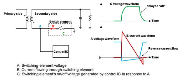
Figure 3: Changes in voltage and current in circuitry surrounding secondary-side switching element (conventional technology)
In this new technology, Fujitsu used a new circuit that controls the timing between the secondary-side control IC and GaN-HEMT. By adjusting the voltage waveform produced by the control IC, the current losses that would normally accompany high-speed operation are suppressed, and current is output with the right timing while taking advantage of GaN-HEMT’s low dynamic resistance. This increases the AC adapter’s efficiency so that it can be made smaller with higher output (Figure 4).
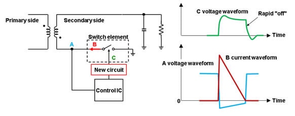
Figure 4: Changes in voltage and current in circuitry surrounding secondary-side switching element (new technology)
Results
As an implementation of this technology, Fujitsu Laboratories built an AC adapter that is compact and fast-charging. In maximizing GaN-HEMT’s properties, wasted power is reduced, enabling it to comply with the Level VI power-efficiency standards for external power supplies that the U.S. Department of Energy will put into effect in February 2016 (Figure 5). Widespread use of this AC adapter would contribute to CO2 reductions.
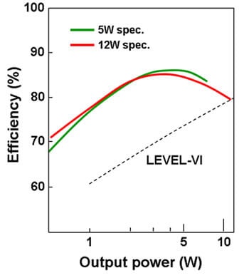
Figure 5: Power output and efficiency of the new AC adapter
Future Plans
Fujitsu Laboratories is continuing to refine this technology, to reduce its size and increase its efficiency, and aims for a practical implementation during fiscal 2017. The company is also looking at higher-output circuits that could extend this technology’s application to notebook PCs.

Leave a Reply
Want to join the discussion?Feel free to contribute!